A linear two-port passive circuit element (no matter how complex) which carries a current between two terminals develops a voltage between these terminals that is proportional to the current multiplied by a complex number, Z, the impedance, or conversely the current to the voltage by Y = 1/Z, the admittance.
The real part of Z is referred to as resistance and the imaginary, reactance. The real part of Y is referred to as conductance and the imaginary, susceptance. The complex numerical nature of impedance is required to describe the fact that current and voltage can be out of phase.
As you know, the simple limiting cases of impedance are wires (zero real and zero imaginary parts), resistance (positive real and zero imaginary), inductance (zero real and positive imaginary) and capacitance (zero real and negative imaginary).
In the following sections we do some exercises to illustrate how the simple circuit components are reborn at RF.
Having read the above sections one can deduce the following laws about Print Circuit Board (PCB.. not Polychlorinated biphenol!) design.
We have the following rule. All radiofrequency circuits in this course will be made on double sided copper PCB with a solid earth plane on the bottom side of the board and all components soldered on the top side of the board. All tracks (or as many as possible) should be designed for radiofrequency operation and be located on the top side of the board. Blank areas between tracks on the top of the board should also be left coppered and frequently soldered to the lower plane. When I say designed for radiofrequency operation, I mean that the track reactance has either been absorbed or resonated (in the narrow band situation) or designed as a transmission line with the lower earth plane as the return conductor.
The only exception to this rule is the case where separate earths may be required. This occurs in mixed signal circuits. Mixed signal circuits are those where both digital (such as TTL and CMOS data usually at 0 - 3 V and 0 - 5 V signalling levels) appear on the same PCB as analog radio signals. Mixed signals are necessary where radiofrequency integrated circuits require computer programming to set their parameters. Examples are frequency synthesiser devices such as phase lock loops and direct digital synthesisers which require their frequencies to be controlled by computer. In this case it is usually wise to observe the above rule but provide for two separate earths connected at one point. The idea is to avoid the noise from sharp transitions in the digital signals from increasing the noise seen by sensitive radiofrequency receivers.
THE EQUIPMENT
The following photographs show some of the equipment and components that are available for use in the course. Students should become comfortable with the operation of the Rohde and Schwarz function generators, the oscilloscopes and the spectrum analyser as these will be routinely used in the project.
In using the FSH-3 spectrum analyser students should attempt the following measurements.
Students should become familiar with resolution bandwidth (RBW) and Video bandwidth (VBW). Have a read of the following information on The Spectrum Analyser. As an exercise try and view the output signal of the SMX function generator.
Learn how to store and recover data on the analyser for off-line analysis. On the lab computers a copy of FSHVIEW is available. There is a serial (/USB) optical cable that can connect the analyser to the computer
In all cases care should be taken with the maximum ratings of the equipment e.g. FSH-3 max input = 20 dBm (100 mW).
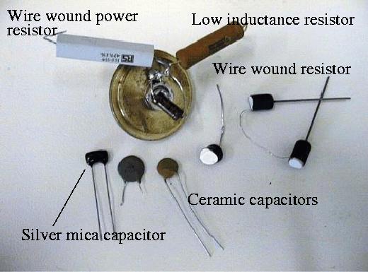
Plate 1. The earth plate for the Vector Network Analyser with a wire wound, a special low inductance and a metal film resistor. At the bottom left are a silvered mica and two ceramic caps from left to right. At the right is a dissected metal film and a wire wound resistor.
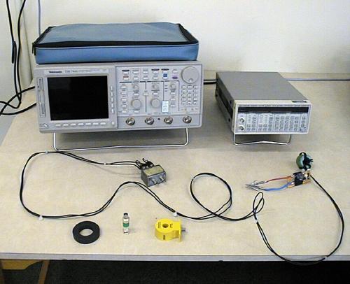
Plate 2. The TDS744A oscilloscope and DS345 function generator. A toroidal ferrite, the current probe and a voltage probe are shown in the foreground.
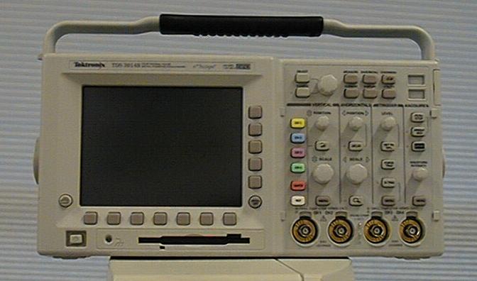
Plate 3. The TDS3014B oscilloscope.
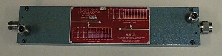
Plate 4. The NARDA 3020B directional coupler.
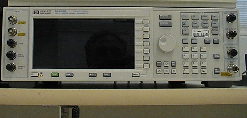
Plate 5. The E4433B signal source is capable of producing up to 20 dBM from .1 - 4000 MHz. It also allows arbitrary IQ modulation and is programmable for some standard schemes such as IS95 CDMA.
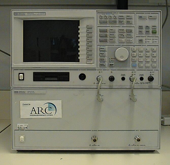
Plate 6. The 89441A vector signal analyser (VSA) allows measurement and demodulation of arbitrarily IQ modulated carriers up to 3 GHz. It can be used to simulate a receiver by demodulating a carrier (for example from the E4433B) after channel effects such as noise and multipath have corrupted the signal. It could also be used later on to check the overall quality of the RF generated BPSK signal.
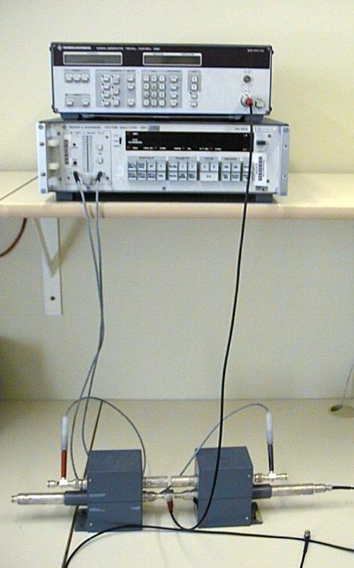
Plate 7. The Rohde and Schwarz SMX signal generator and ZPV Vector Network Analyser (VNA). Down the bottom are a pair of directional couplers used to sense reflected signals from an open circuit load and a DUT (Device Under Test). From these signals, the ZPV computes impedance of the DUT.
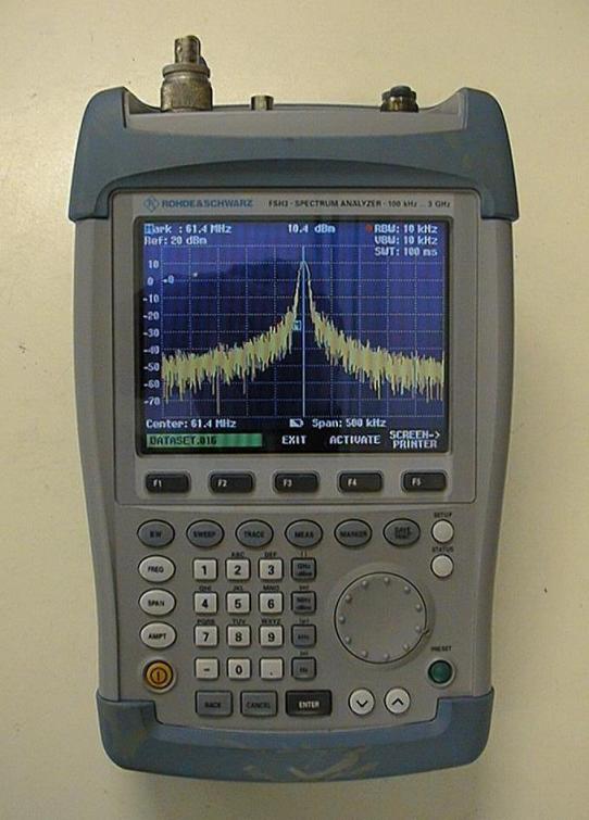
Plate 8. The Rohde and Schwarz FSH-3 spectrum analyser. Spectrum analysers plot the scalar frequency spectrum of input signals. The input shown at the right is terminated in 50 Ohm. The connector on top to the left is the signal input and the connector to the right is for the tracking generator. The tracking generator provides a swept signal source for test purposes such as the measurement of the scalar transfer function of a filter. We have options for this analyser which allow remote control and vector analysis. With the latter option the spec an is literally a VSA or VNA and can therefore be used to measure impedance.
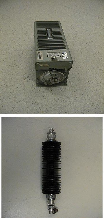
Plate 9. A 500 Watt and a 5 Watt attenuator.