next up previous contents index

[ENGN2211 Home]

Amplifier

The DC operating point Q for a JFET amplifier is frequently chosen so that

 \begin{displaymath}I_D = \frac{I_{DSS}}{2}
\end{displaymath} (118)

i.e. midway in its operating range.

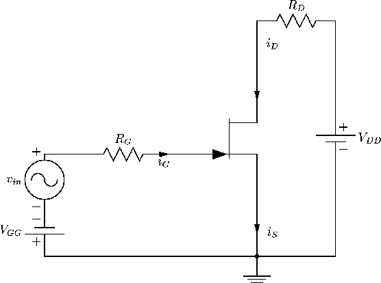
Now let's add an AC voltage source to the circuit of Figure 123, as in Figure 130 (this is not a practical amplifier circuit, it is used here for illustration only).


Figure 130: n-channel JFET as an amplifier.
\begin{figure}
\begin{center}
\epsfig{file=images/fetimg12.eps}\end{center}\end{figure}

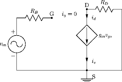
We use the AC small signal model of Section 9.3.2, which we use to re-draw the circuit of Figure 130, see Figure 131.


Figure 131: AC equivalent circuit.
\begin{figure}
\begin{center}
\epsfig{file=images/fetimg13.eps}\end{center}\end{figure}

Now since ig=0, we have vg=vgs=vin. Then gm vgs = gm vin, and by KVL,
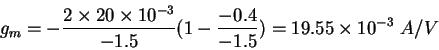
vd = - id RD = - gm RD vin

and so the gain is given by

 \begin{displaymath}A = \frac{v_d}{v_{in}} = -g_m R_D .
\end{displaymath} (119)

This gain is negative, and depends on the transconductance gm. The amplifier is an inverting amplifier.  

Example. Let RD=1.2 k$\Omega$, VDD=30 V, VGG=-0.4 V, with the JFET parameters IDSS=20 mA, Vp=-1.5 V. Then VGS=-0.4 V, so

\begin{displaymath}I_D = 20 \times 10^{-3} (1-\frac{-0.4}{-1.5})^2 = 10.76 \ mA
\end{displaymath}

and

\begin{displaymath}V_{DS} = 30 - (10.76 \times 10^{-3} )(1.2 \times 10^3) = 17.1 \ V
\end{displaymath}

This defines the DC operating point Q.

The transconductance is

\begin{displaymath}g_m = - \frac{2 \times 20 \times 10^{-3}}{-1.5}(1-\frac{-0.4}{-1.5})
= 19.55 \times 10^{-3} \ A/V
\end{displaymath}

and so the amplifier gain is

\begin{displaymath}A= - (19.55 \times 10^{-3})(1.2\times 10^3) = -23.47
\end{displaymath}


next up previous contents index

[ENGN2211 Home]

ANU Engineering - ENGN2211