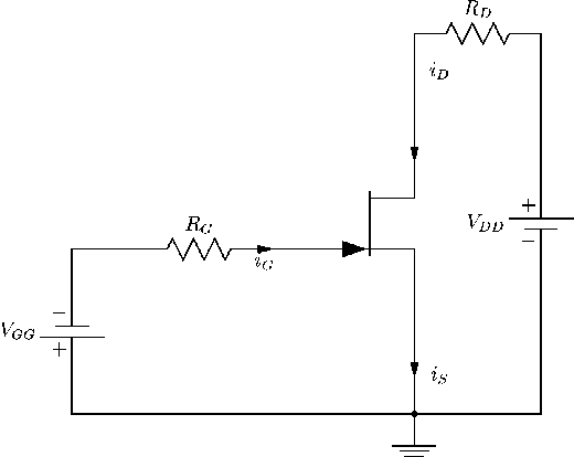
The circuit of Figure 123 will be used to study the JFET characteristics. The JFET is a nonlinear device. The voltage sources VGG and VDD will be adjusted.
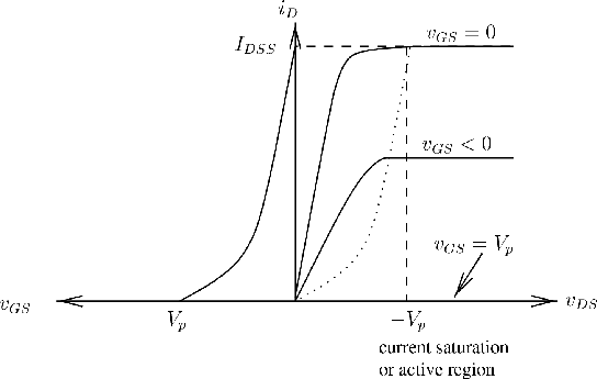
A graph of the JFET characteristics, iD versus vDS and iD versus vGS is shown in Figure 124.
Consider first vGS=0 V. For small values of vDS, the drain current iD increases linearly. For larger values, the increase of iD is nonlinear until pinch-off occurs when vDS reaches the value -Vp. After pinch-off, iD cannot increase further, and stays constant at the value IDSS.
Now decrease vGS to a negative value. Then pinch-off
occurs at a lower value of vDS, indicated by the doted
line. After pinch-off, in the active or current saturation
region, the value of drain current is given (approximately)
by the square law
If vGS is reduced to the negative value Vp, then iD=0 and current flow is cut-off.
Note that, according to (110), iD is
a quadratic function of vGS.
The shape of the iD versus vDS characteristic is similar
to the iC versus vCE curve for a BJT, Figures
97 and 98.
However, in the case of the BJT
![]() in the
active region, a linear relationship (although
in the
active region, a linear relationship (although
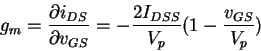
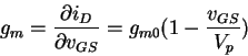
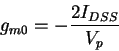
An important parameter is the transconductance gm
defined by
ANU Engineering - ENGN2211