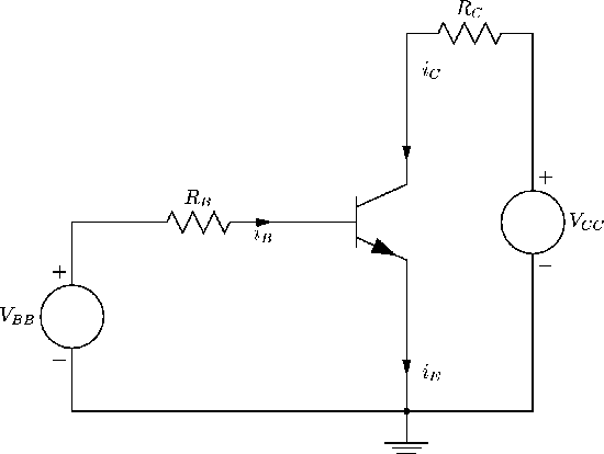
Consider the circuit of Figure 96, which we will use to learn about the operation of the transistor in a circuit by adjusting the voltage sources VBB and VCC.
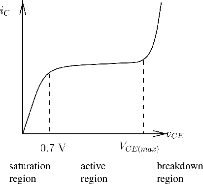
A graph of the collector characteristic, iC versus vCE is shown in Figure 97.
Suppose VBB and VCE are set to produce a current iB > 0 and VCE=0 V. Then both BE and BC junctions are forward biased. The saturation region corresponds to the case where both junctions are forward biased.
As vCE increases and
reaches about 0.7 V, the BC junction becomes reverse biased
(before this, the transistor is in saturation).
When vCE exceeds 0.7 V, the transistor goes into
the active region, or linear region
corresponding to the BE junction forward biased and BC reverse biased.
This is the normal mode of operation of the transistor, e.g. as in
amplifiers. In the active region the collector characteristic is almost
flat, meaning that iC is almost constant but vCE can vary.
The value of iC is determined by iB,
If vCE increases too much, the transistor goes into the breakdown region. This should be avoided.
Figure 98 shows collector curves for different values of base current. When iB=0 A, the transistor is in its cutoff region , and only a small leakage current flows as iC.
ANU Engineering - ENGN2211