next up previous contents index

[ENGN2211 Home]

Introductory FET Circuits

Consider again the circuit of Figure 123. We first do a DC analysis using the DC model of Section 9.3.1. You can either re-draw the circuit subsituting the model of Figure 127 for the transistor, or simply keep the same diagram and write explicitly the algebraic equations

 \begin{displaymath}I_G=0, \ \ \ I_D = I_S = I_{DS}= I_{DSS}(1- \frac{V_{GS}}{V_p} )^2
\end{displaymath} (115)

corresponding to the DC model.

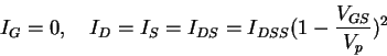
Since IG=0, the voltage drop across RG is zero, and so VG = VGS=-VGG; i.e. the gate-source voltage VGS is determined directly as -VGG due to the left voltage source. Now IDSS and Vp are given parameters of the JFET, and so the drain current ID can be determined from (115).

Next, KVL gives

VDD = ID RD + VDS

and therefore VDS is given by

 
VDS = VDD - ID RD . (116)

This determines the operating or quiescent point Q.    

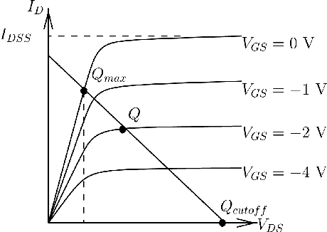
Graphically, we can plot the load line  

 \begin{displaymath}I_D = \frac{V_{DD} - V_{DS}}{R_D} .
\end{displaymath} (117)

on the ID-VDS characteristic, the intersection with the curve corresponding to the value of VGS giving Q, see Figure 129.


Figure 129: JFET load line.
\begin{figure}
\begin{center}
\epsfig{file=images/fetimg11.eps}\end{center}\end{figure}


next up previous contents index

[ENGN2211 Home]

ANU Engineering - ENGN2211