Semiconductor materials such as silicon (Si) and galium arsenide (GaAs) are crystals formed from the sharing of four valence electrons in covalent bonds. The energy gap between the valence level and the conduction level is midway between that of insulators and conductors (such as metals), and thermal energy causes electrons to leave the valence state and change to a conduction state. When an electron reaches the conduction level it leaves a hole in the valence level. Electricity is conducted via the flow of electrons and holes. In a pure crystal the number of conduction electrons equals the number of holes and this number is rather small at room temperature. Recombination refers to the return of an electron to the valence level (since a conduction electron-hole pair is combined).
The conduction characteristics can be changed by a process of doping. An n-type semiconductor has a small amount of impurity added. This impurity, called the donor (e.g. P, As, Sb) has a valence of +5, and four of these electrons are used in the covalent bonding while the fifth electron is readily excited to the conduction level. In a n-type semiconductor, the number nn of conduction electrons is much larger than the number of holes pn ( nn >> pn). Electrons are the majority carriers and holes are the minority carriers.
In a p-type semiconductor, the impurity is called an acceptor (e.g. B, Ga, In) and has a valence of +3, and all electrons are used in covalent bonds. This results in conduction holes. In a p-type semiconductor, the number pp of holes is much larger than the number of electrons np ( pp >> np). Holes are the majority carriers and electrons are the minority carriers.
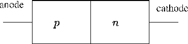
The pn junction is an interface between a p-type and an n-type region and is used to construct diodes and transistors. A diode consists of a single pn junction, Figure 68.
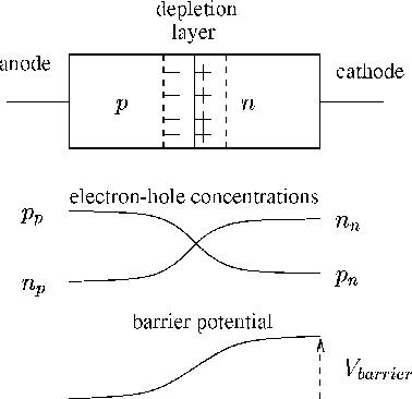
At the junction, majority carriers diffuse across the junction, and this creates a depletion layer and a barrier potential Vbarrier across the junction. The voltage Vbarrier causes an opposing current flow, and the two flows form an equilibrium. This is illustrated in Figure 69.
 |
ANU Engineering - ENGN2211