[ENGN2211 Home]
DC Bias
Load the PSPICE file
jfet-dc3.sch,
Figure 45.
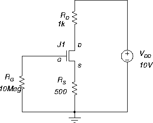
Figure 45:
Circuit for JFET DC operating point (self bias).
 |
Exercise:
- 1.
- Examine the self bias circuit of Figure 45
and calculate VG, VGS, ID and VDS and VD
using the relations
VGS = -ID RS ,
(Use RD=1 k ,
RS=500 ,
and the values
of IDSS and Vp you determined above.)
,
RS=500 ,
and the values
of IDSS and Vp you determined above.)
- 2.
- Simulate the circuit for the given setup.
Is the transistor J1 in the active region? Why?
- 3.
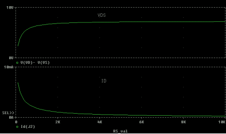
- We now wish to investigate the effect of varying
the source resistor RS on the DC operating point,
and in particular on ID and VDS.
We do this using DC sweep, with RS
set up as a parameter, varying between
100
and 10 k.
Enable DC sweep and simulate again.
Obtain plots of ID and
VDS=VD-VS vs RS
(similar to Figure 46).
- 4.
- Explain what you see.
Note carefully the effect of RS on ID and VDS.
- 5.
- Draw load lines on the characteristic graphs (ID vs VDS) for three values of
RS: 0.1, 0.5 and 1.0 k.
The horizontal intercept is VCC=10 V, and the vertical intercepts are given by
Plot the operating point Q corresponding to item 1 (on the RS=0.5 k
load line).
These results can be used for the amplifier of the next section.
Figure 46:
DC operating point varies with RS.
 |
[ENGN2211 Home]
ANU Engineering - ENGN2211