next up previous contents

[ENGN2211 Home]

Switching and Load Line

Load the PSPICE file jfet-dc2.sch, Figure 42.


Figure 42: Circuit for JFET switching and load line.
\begin{figure}
\begin{center}
\epsfig{file=images/clab7img4.eps}\end{center}\end{figure}

Exercise:

1.
Try to calculate VGS, VG, ID and VD=VDS using the DC model for the JFET. (assume IG=0 A) for the circuit of Figure 42 (use VDD=10V, RG=50 k$\Omega$, RD=3.3 k$\Omega$).

Simulate and compare with your calculations.

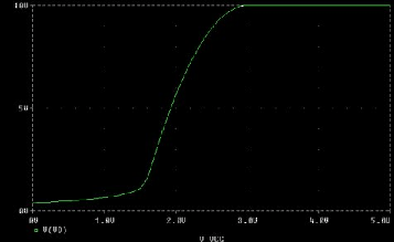
In your calculations, use the parameters IDSS and Vp you measured above.

Are the assumptions for the use of the DC model valid? Explain.

2.
Enable DC sweep and simulate again, to obtain the graph of Figure 43 showing the switching characteristic (VGG varies between 0 V and 5 V). At what value (approx.) of VGG does switching occur? Discuss.

3.
Obtain the load line of Figure 44 from the same simulation.

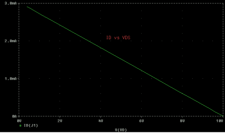
In this case, the load line is given by

\begin{displaymath}I_D = \frac{V_{DD} - V_{DS}}{R_D}
\end{displaymath}

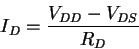
This is easy to sketch on your printout, by first determining the x and y intercepts.


Figure 43: JFET switching curve.
\begin{figure}
\begin{center}
\epsfig{file=images/clab7img5.eps}\end{center}\end{figure}


Figure 44: JFET load line for the circuit of Figure 42.
\begin{figure}
\begin{center}
\epsfig{file=images/clab7img6.eps}\end{center}\end{figure}


next up previous contents

[ENGN2211 Home]

ANU Engineering - ENGN2211