next up previous contents

[ENGN2211 Home]

Small Signal Amplifier

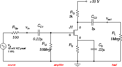
Load the PSPICE file jfet-amp1.sch, Figure 47. Your task is to a design value of RD for the best compromise between good gain and output voltage swing.


Figure 47: Small signal JFET amplifier.
\begin{figure}
\begin{center}
\epsfig{file=images/clab7img9.eps}\end{center}\end{figure}

Exercise:

1.
Choose a (standard) value of RS so that the DC operating point is such that $I_D \approx I_{DSS}/2$ (approx.). Set in PSPICE.

You may use your curves from the DC bias exercise above, section 8.4.

2.
Simulate and check the DC bias is correct.

Draw the load line on the characteristic graph (ID vs VDS) for your value of RS. Plot the DC operating point Q on this load line.

Check for consistency with the DC bias exercise above, section 8.4.

3.
Calculate the gains Ain,out and As,out.

Lecture Notes : FET Transistor Circuits : Small Signal Amplifiers

4.
Enable transient analysis and simulate. Determine from your simulations results the AC gain As,out. Compare with theory.

To measure the gain, measure the peak-to-peak values of vs and vout and calculate the ratio vout/vs.

5.
Experiment with different values of vS, RSo and RL and note the effects. Discuss.


next up previous contents

[ENGN2211 Home]

ANU Engineering - ENGN2211