In this section we look at the design of a 1 Watt FET power amplifier using the 2N7000 n-channel enhancement mode MOSFET. We will cover four possibilities with class A, C, E designs and a suggestion for a class B design. Class A means that the transistor is biassed to about the mid supply on its drain with quiescent current. In class A we aim to use the full linear range of the transistor. In class B the transistor is in partial conduction with no signal but will be cutoff when the input signal is sufficiently negative. In class C the FET is conducting for less than half of the input conduction cycle. Class E is one of several switching mode designs. Classes C and E cannot tolerate linear amplitude variations and in the VHF wireless project the use of BPSK or FSK is consistent with this choice. I should say from the outset that the only reason that I chose the 2N7000 for these applications is because it is a really cheap (AUD0.80) FET capable of 400 mW power dissipation. This could be a rather slow transistor so we will have to take care with the designs, particularly class E. My guess is that it is not too bad.
WARNING: It will not be possible to make a 1 Watt class A power amplifier with one 2N7000. You will need several FETs. At AUD0.80 this is NOT a problem and there are quite convenient ways of combining many parallel amplifiers.
Although I could calculate the S-parameters, we do not need them for power amplifier design. For PAs we use device capacitances in the data sheet. This is somewhat akin to the approach I took to compute the S-parameters from these capacitances in the chapter on small signal transistors. I have not found S-parameter measurements for this transistor conveniently available on the web anyway (may be we should do some measurements if the 2N7000 turns out to be a success:). The 2N7000 is however low cost and one can try to obtain more power in any design by increasing the drive level, putting several of the FETs in parallel (unlike BJTs, FETs are well suited to being stacked in parallel because of their negative current vs temperature characteristics.. i.e. unlike BJTs, FETs do not suffer from thermal runaway) and other tricks you may imagine. The latter advantage may allow us to go to a ridiculous power supply voltage like 5 Volts! (obviously this would be nice).
Note that I have specified the drive level as 20 dBm for the modulator/TR student group so you will have to make up the difference. Note also that the class C and E designs will require a comparator drive anyway and you'll have to supply this anyway (NE521.. look it up on the web!).
PROJECT 1: CLASS A DESIGN AND CONSTRUCTIONLet's look at a class A design. It is 1 Watt PA based on the 2N7000 N-channel enhancement mode MOSFET. The following figure shows the complete circuit. Although it looks complete it is only a suggestion. I anticipate bias problems if things turn awry. So we'll have to look at bias stabilisation techniques (maybe, or neutralisation of oscillations).

In this example we'll treat one such amplifier. Of course you can build a couple of identical amps that can be driven in parallel as well as reworking this design with several FETS connected gate-to-gate, drain-to-drain and source-to-source. (if your are not familiar with these terms please look up the datasheet or a text book). If you do the latter then you must be very careful to do the design. In this way you might be able to consider using a 5 V supply instead of the 12 V and you must do so in order to achieve 1 Watt. Then at the end I'll describe an incredibly robust and simple technique for combining these identical amplifiers based on the quadrature phase hybrid so that they can be guaranteed never to interact adversely.
The procedure to design a class A is the following.
- Obtain the input and output capacitances of the FET.
- Find the optimal load impedance from the load-line required do deliver the desired power to the load.
- Design matching networks to match to 50 Ohm at the input and the output.
Note that the last step you already know about. Please make sure you understand all about matching networks.
The first step is to obtain the 2N7000 data sheet. The following figure shows the capacitances of the FET.
In the above figure gm is the FET transconductance. Note that this is a small signal model but we do not use it: it is only here for illustration purposes to show where the capacitances are. For the 2N7000, the capacitances but no resistances are listed in the data sheet. Why should there be resistances? I guess that for FETs the drain-source resistance is the only one of interest since it can be quite low. However the effect of resistance is already taken into account in the load-line analysis of the FET that follows shortly. The capacitances on the other hand are not already present in the load line analysis and must be separately treated (using a matching network to eliminate their effect at high frequency).
The electrical characteristics table in the data sheet gives the gate to source capacitance, CGS = 20-50 pF and the drain to source capacitance CDS = 11-25 pF. These have quite a large uncertainty which will have to be taken into consideration when doing the design. The drain to gate capacitance CDG is 4-5 pF and is not negligible especially as it will be amplified by the Miller effect. It could also lead to instability and might have to be neutralised.
The following figure shows the IV characteristics of the FET. These are the transfer and output characteristics of the FET taken from the data sheet. Note that the gate to source voltage (VGS) is what drives the FET. This produces excursions in the drain to source current (IDS) which in turn produces the output voltage swing by varying the drain to source voltage (VDS).
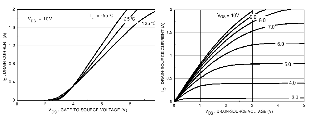
We assume that the load resistance that we require is that which gives our desired power for the maximum possible excursion of the output voltage VIZ RLOAD = (VDS - Vsat)2/(2P). Vsat is the minimum value that the drain-source voltage can have from the IV characteristics. The first thing to understand about class A is that we will be biasing the circuit in such a way that the output produces the complete excursion of a sine wave as best it can for the given power.
The following circuit shows the output excursion for maximum power transfer assuming that Vsat = 0. We will also use this figure to discuss the non-linear high efficiency modes (class AB,B and C) in a little while. We use a choke (DC resistance equal to zero) to connect the drain to the power supply so that the DC bias on the drain is equal to the supply voltage (VCC). Optimum power transfer will occur when the load resistance (which is seen here absorbing CDS in the output matching network) has the right value to make the peak current excursion equal to (VCC -Vsat)/ Rload. Larger amplitude swings than this are not possible because under no circumstances can a FET (or a BJT) with a supply between ground and a positive value ever conduct negative current.
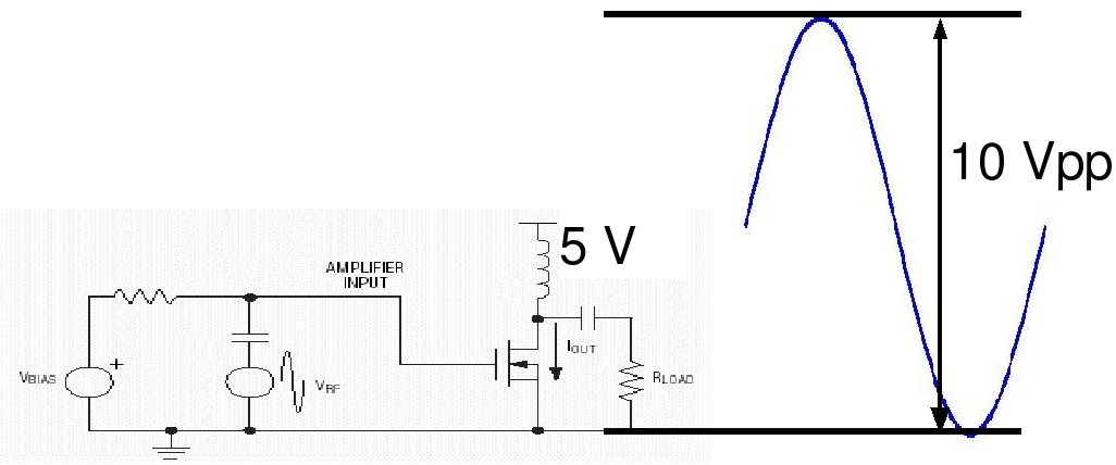
Dont forget that we are assuming that the matching network is already functioning in order to produce the RLOAD. This is why we are hiding the fact that there is a CDS = 25 pF.
Remember that we cannot do this design for 1 Watt for a single amplifier because in class A, RLOAD and the FET dissipate the same power and 1 Watt EXCEEDS the power rating of the 2N7000.
The DC voltage on the drain, VDS (under no excitation) must be VCC. The minimum value of VDS is Vsat. The maximum peak excursion on the drain is VCC + VCC - Vsat = 2VCC - Vsat and the peak-to-peak swing is 2(VCC - Vsat). The peak current into the load is ILOAD = (VCC - Vsat)/RLOAD and this must be achieved when the drain current is zero Id = 0.
The voltage across the load, Vt at any time is given by,
Vt = (VCC - Vsat)/RLOAD sin(Wt)
The current across the load, It at any time is given by,
It = Vt / RLOAD
Because the blocking capacitor has a quiescent voltage VCC across it, the drain voltage is given by,
VDS = VCC + Vt
The current in the power supply choke is a constant and is given by the load current when the FET is cutoff as follows,
ICHOKE = (VCC - Vsat) / RLOAD
On the negative half cycle of Vt the drain current is sourced from the decoupling capacitor which acts as a kind of power supply in this circumstance with an equal current from the choke and is given by,
max(IDS) = 2*(VCC - Vsat) / RLOAD
The minimum value of IDS occurs when the drain voltage reaches its peak and is,
min(IDS) = 0
Thus IDS is given by
IDS = (VCC - Vsat)/RLOAD - Vt/RLOAD;
Finally we can write the load line which is the relationship between IDS and VDS,
IDS = (2VCC - Vsat - VDS)/RLOAD;
Some MATLAB code that does this for you is appended at the end of this page.
If we want 0.25 Watt of power for a 5 Volts supply then using the above formula and guesstimating Vsat = 0.2 Volts from the above IV-characteristics we obtain the following load line,
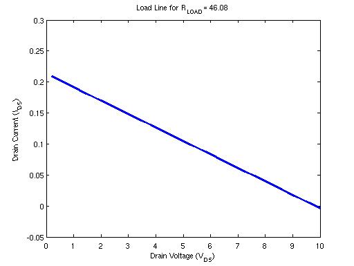
Note that this produces an accidently convenient value of RLOAD = 46 Ohm. Since this may as well be 50 Ohms we have a trivial matching task and may as well use any old Chebyshev low pass filter to match to the antenna preselector (50 Ohms). Note that you still need a matching network because you still need to absorb the 25 pF of CDS capacitance.
To match the input you just use the matching techniques to match the 20 dBm signal from a 50 Ohms source to the input impedance. Notice that the input impedance of the FET is just CGS = 50 pF in parallel with R1 = 68 Ohms in the simplified figure below. The actual value of R1 is determined entirely by the bias to get the FET into the class A regime from the above IV-characteristics. Because CGS is so large (-j80 Ohms at 40 MHz), the real part of the parallel combination of CGS and R1 is divided down any way.

Have a look at this section for an example on how to use matching techniques in the design of a class A amplifier.
One could attempt a class-A design with the MRF134. We have a few of these lying in old amplifiers in the lab and you are free to use them. If you miss out then have a look at RS stocks . Note that not all of these are RF trasnsistors.
If you do try to do a class-A design (or a class-B) then you will also need to build a few hybrid couplers and these will need to be modeled first. Information about these is provided in the next section.
Combining Power Amplifiers
The problem with the class A design above is that the 2N7000 is not capable of dissipating 1 Watt. One solution to this problem is to combine a number of identical amplifier stages as follows,
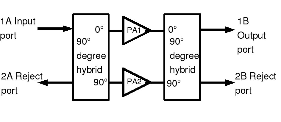
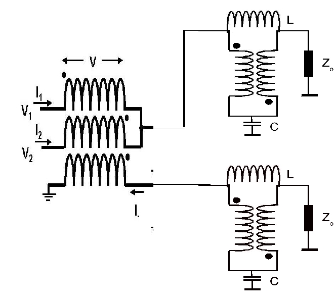
The essential component that allows this is a couple of 90o phase hybrids. The devices will soon be described in the section on transmission line transformers, but a quick intro is in order here. The essential component in the discrete version of the phase hybrid is the circuit shown in the following diagram. Each phase hybrid uses two of these.
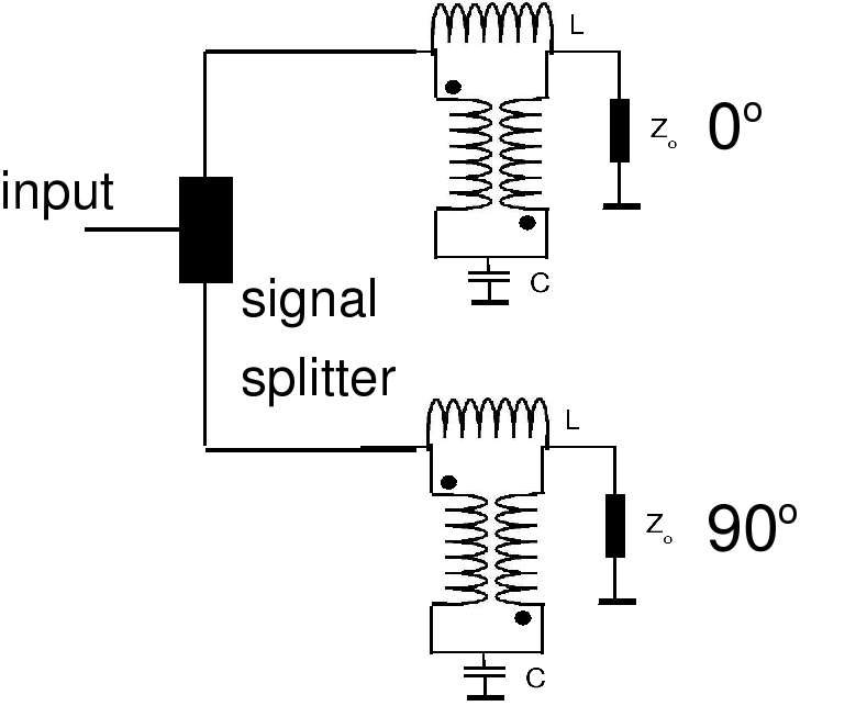
The following figure expands this schematic to show the specifics of the power coupler.
PROJECT 2: CLASS AB, CLASS B AND CLASS C DESIGNS
As we saw in the above example, we are not going to achieve a simple class A design with the 2N7000 because we will need four of them combined to achieve the desired 1 Watt power requirement. You may however wish to try the MRF134 instead if there are any left in the lab :).
There are howver non-linear high efficiency modes referred to as classes AB, class B and class C. These are the classical high efficiency modes. The essential difference between these non-linear high efficiency modes anf class A is that the negative sine wave excursion of the drain (or collector) current now pinches off as shown in the following figure. These show the current waveforms for class A (blue), class B (red) and class C (black). The problem with class A is that the amount of power dissipated in the transistor is equal to that dissipated in the load. This is entirely unnecessary as shown in the figure. What happens is that the conduction angle of the current in the transistor decreases as the bias in the input circuit is reduced. Intuitively this improves efficiency however it also reduces the actual output power. Thus these high efficiency modes need increased drive.
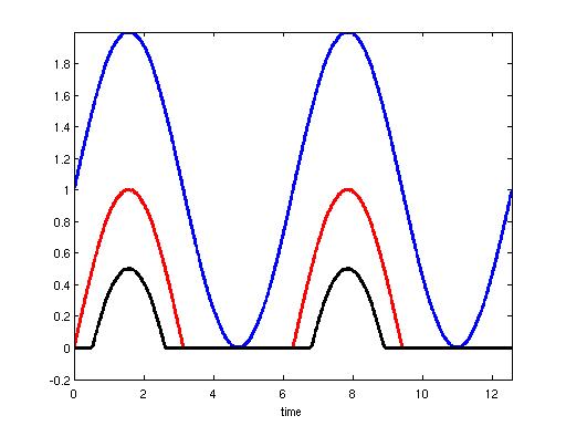
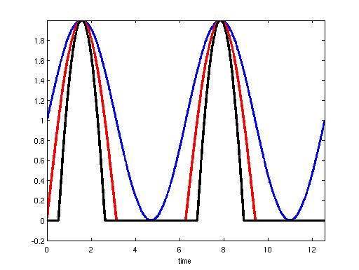
The obvious consequence is that the quiescent voltage as a fraction of the power supply voltage decreases with reduced input bias. Therefore one has to replace the lost DC input bias by increased input drive to the point where the peaks of the currents in class B and C peaks out at the peak level Imax of class A as shown in the following figure.
Note that Imax is not just a property of class A. So what is Imax exactly? We will assume that Imax is determined by the required output power in class A. This may seem strange as one would think that a transistor driven in class A would be limited in the values of Imax that it could produce and obviously this is the case. In fact we choose Imax such that, Imax = 4P/VVcc where VCC is the power supply voltage and P the desired output power (class A only). We are choosing Imax to give the maximum power in class A. Indeed, class A is the mode that allows the maximum power to be produced. As we shall see, the non-linear modes produce less power but with much higher power supply efficiency and at significantly higher input drive. Power supply efficiency refers to the ratio of out to power supply power and obviously ignores input stage drive power. Now getting back to the choice of Imax: there is no problem with the above maximal power choice as we still have to compute the drive that will produce it. Moreover, a particular choice of output power and hence Imax exceeds the ratings of the transistor such as device dissipation then we will obviously have overstepped the mark and attempted to draw too large a value of Imax. This may not matter if we are only using this value of Imax to do a design for a higher efficiency class as we shall see. If it is a class A design however then we will just have to reduce the required output power or find a more powerful transistor.
From the figure the negatve current excursion is also limited. This is because of the fact that the transistors cannot conduct in the reverse direction.
There is no fundamental limit on the voltage excursion Vs but we will try to limit it to 2VCC, the power supply voltage. Note that PAs will always have a choke in the drain (collector) to power supply line so that the output voltage excursion can reach double VCC. The effect of the choke is to minimise current variations in the output circuit from reaching the supply and therefore acts like a DC current source whose current is switched between the transistor and the load. The switching waveform is not that of a normal switch however, but a switch whose current waveform in the transistor is determined by the drive and looks like the half sinusoids in the above figure
A couple of programs have been written to help picture these waveforms and compute the powers at least for the cases where we ignore the knee of the IV characteristic and the saturation voltage. The first is PAOUT.m which integrates the current through the choke for a load which produces the maximum power. The conduction angle in these is denoted alpha.
The formal definition of the classes is shown in the following table. The bias point is the quiescent voltage on the drain (collector). Here it is measured as a ratio of VCC. Note that class A is biased at half the supply and class B at zero output volts. The quiescent drain (collector) current is measured here with respect to Imax. As expected in class A the current is biased at half of the peak excursion Imax and class B at zero. Notice that class C cannot be negative!!.
| Class | Bias point |
Quiescent Current | Alpha |
| A | 0.5 | 0.5 | 360 |
| AB | 0 -> 0.5 | 0 -> 0.5 | 180-360 |
| B | 0 | 0 | 180 |
| C | <0 | 0 | 0-180 |
The file classes.m computes the efficiency (defined as power into the load over power from the supply). The following figure shows a plot of efficiency (0-1, blue), device dissipation (red) and Pout (green) in Watts and the optimal Rload (ratio to that in class A) (constrained to the fact that the voltage excursion is 2Vcc) (black) ( I am not sure why this is necessary in fact as it cannot be true in switch amplifier modes such as class E (See "RF power amplifiers for Wireless Communications" by Steve C Cripps (Artech House) for more information (perhaps)). The Rload and power values assume that the power supply is 5 Volts and the power into the load is 1 Watt. Note that this is used to estimate Imax from the relation Imax = 4P/VVcc in class A. This means that we calculate Imax on the basis of the current required to deliver the desired power (here P = 1 Watt) in to a load. But this power is only that for class A. The Rload value for class A of course is therefore given by Rload = Vcc^2/2/P = 12.5 Ohms. Note that Imax is the peak excursion of the transistor current starting at a lowest value of 0 and corresponding to the complete excursion of VS the drain (collector) voltage. (i.e.10 Volts here as shown in the previous figure for class A.
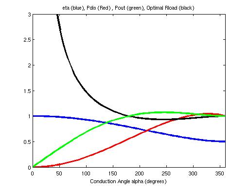
This figure already contains a few surprises. Firstly the possible output power in class B is the same as that in class A. In fact the power remains approximately constant for alpha from 0o to 180o. The power into the load tends to drop significantly for conduction angles lower than that of class B whilst the efficiency increases dramatically. So for example while class A has an efficiency of only 50%, class B is about 78% per cent efficient. Whilst class C with alpha = 90o is about 98% efficient. Class B has just over 50% of the device dissipation as class A for the same output power.
An interesting exercise therefore is to consider the design of a class B power amplifier. Since the 2N7000 can dissipate 400 mW, then it should now be possible to consider just two class A amplifiers with the bias adjusted back to just cause drain (collector) current pinch off. These can then be combined in parallel using the phase hybrid described above.
PROJECT 3: A 20W PA BASED ON THE PHILIPS BLF245 ENHANCEMENT MODE MOSFET
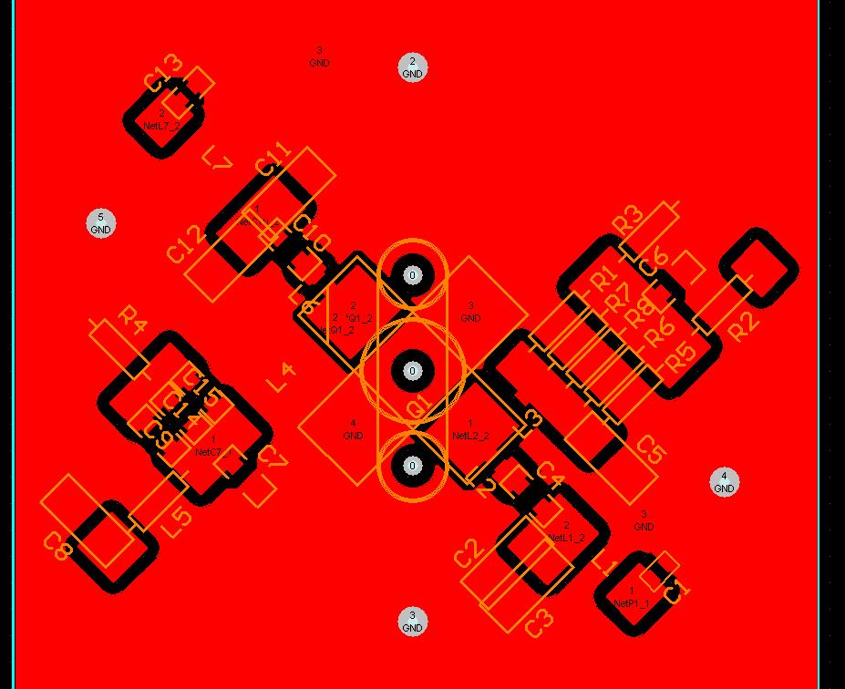
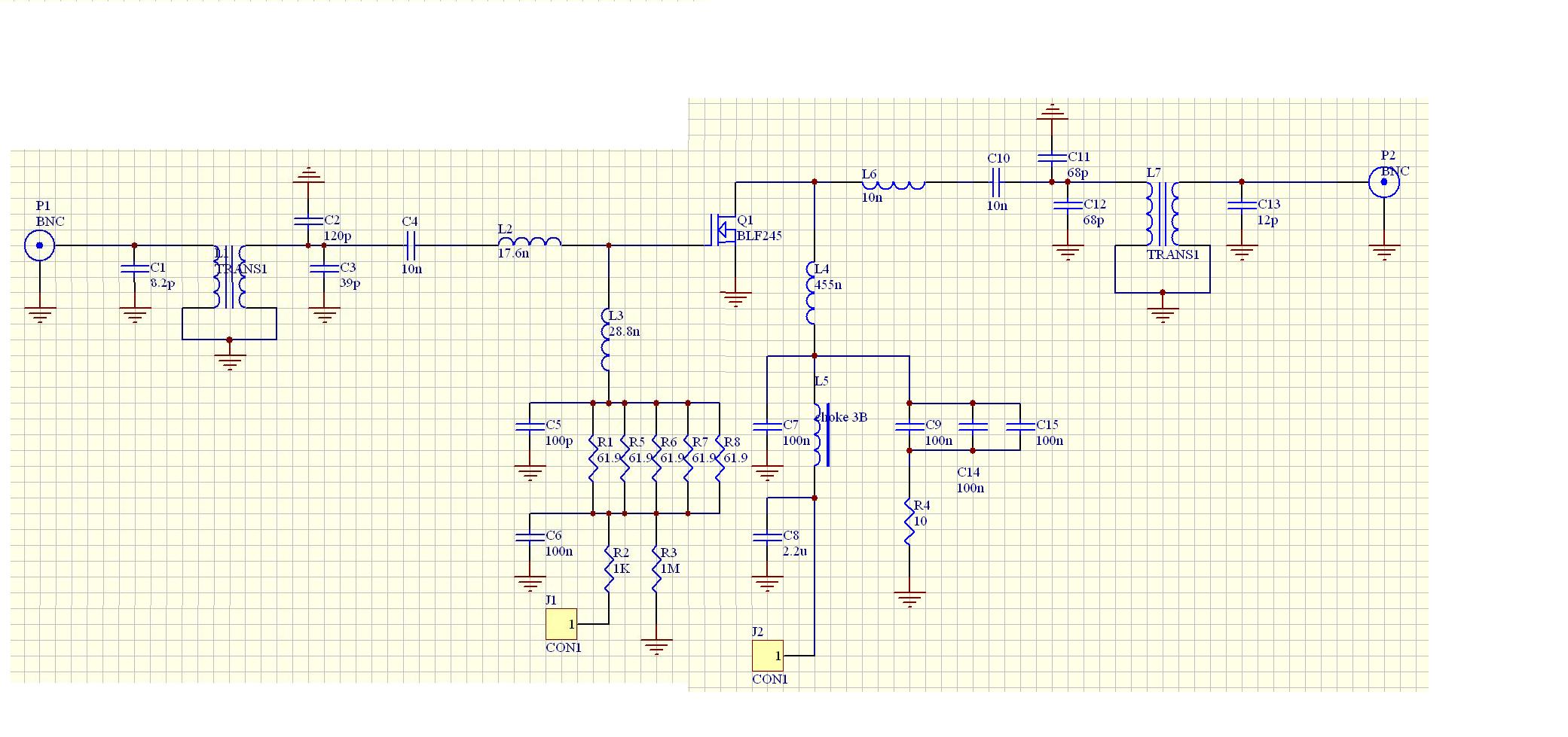
The following document describes an alternative amplifier. This is a 20 Watt 25 - 100 Mhz amplifier that suits me for my other projects. We have enough resources including a circuit board for this design. The following figure shows the circuit layout under construction.
MATLAB CODE TO DO CLASS A LOAD LINE CALCULATIONS
clear all
close all
%The power level we want..
P = 0.25 %Watt
Vcc = 12;
Vsat = .2;
Vd = linspace(Vsat,2*Vcc,50);
RLOAD = (Vcc-Vsat)^2/2/P
Id = (2*Vcc - Vd - Vsat)/RLOAD;
figure(1)
plot(Vd,Id,'LineWidth',3)
xlabel('Drain Voltage (V_{DS})')
ylabel('Drain Current (I_{DS})')
title('Load Line for R_{LOAD}=72 \Omega')
Pdis = max(Vd.*Id)
t = linspace(0,1,100);
%NB dc operating point is Vdc = (2Vcc-Vsat)/2 + Vsat = Vcc + Vsat/2
Vt = (Vcc-Vsat)*sin(2*pi*t);
It = Vt/RLOAD;
Vds = Vcc + Vt;
Ids = (Vcc - Vsat)/RLOAD - Vt/RLOAD;
%PLOAD across the load resistor
PLOADt1 = Vt.*It
PLOADt2 = Vt.^2/RLOAD
PLOADav = mean(PLOADt1)
%The FET drain current
PFETt = Vds.*Ids;
PFETav = mean(Vds.*Ids)
figure(2)
plot(t,PLOADt1,'k',t,PLOADt2,'bo',t,PFETt,'r','LineWidth',3)