In networks we learned that
maximum power transfer from source to load occurs when the output
impedance of the source is equal to the complex conjugate of the
impedance of the load. The output impedance is that appearing in the
Thevenin (or Norton equivalent circuits). Here we apply this rule to
the design of LC matching networks used for the matching of a source
impedance to a load impedance. We only cover a fraction of the
matching network possibilities here (for further reading see Bowick).
Matching networks guarantee maximum transfer of power from a source to
a load. As a result they appear everywhere even for matching one
amplifier stage to another. First however we learn the elementary
facts about reactances and resonant circuits.
RESONANT CIRCUITS AND Q
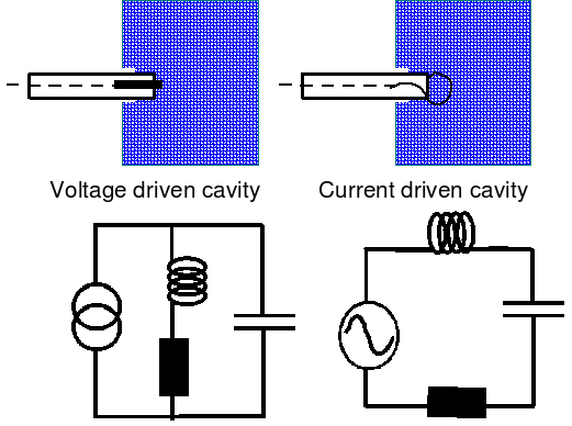
As we saw in the chapter on
impedance, L's and C's have internal losses. If a perfect L and a
perfect C are connected in series then at resonance their impedance is
zero. If they are connected in parallel their impedance is infinite.
Clearly neither is the case if either the L or the C has losses.
Reactances that have internal losses are often described by the term
lossy. Moreover, even perfect L's and C's used in matching
networks involving resonant circuits between resistive source and load
impedances are loaded by these resistors.
A useful quantity to describe the loading effect on a
component is the Q. The Q of a perfect reactance, X, connected in
series with a loss resistance R is defined as Q = X/R. If the loss
resistance R' is connected across the reactance X' then Q = R'/X'.
The physical meaning of Q is exposed through the following formula,
Q = &omega (Energy Stored in X)/(Power lost in R)
By the energy stored we mean the mean oscillating
electromagnetic signal energy present in the reactance under
excitation while the power lost is dissipated in the resistance.
For a perfect lossless reactance Q is infinite. One way to
measure Q at a particular frequency, is to connect the reactance under
test in series with a lossless reactance of opposite sign at that
frequency and resonate the two by scanning the signal frequency around
the centre frequency as shown in the following figure.
The measured curve would look as follows,
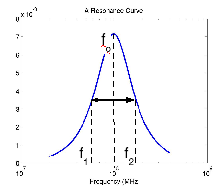
The Q is obtained by the formula Q =
fo/(f2-f1) where f1 and
f2 are the 3dB frequencies or the frequencies where the
signal power in the lossy reactance drops to a half on either side of
the resonant frequency. The resonant frequency is that at which the
reactance looking into any of the above circuits is zero. Thus the
bandwidth of the circuit is determined by Q.
Notice that Q is quite a general quantity capable of characterising
lumped reaactances such as inductor and capacitor components as well
as resonant cavities. It is also a useful quantity. As we shall see Q
directly determines the stopband rolloff of certain filters. We now
use it to design matching networks.
Ex 9. Derive an expression for the Q of a reactance if R' appears in
parallel with X'. I.E. Prove that Q = R'/X'.
Ex 10. Show that R' = (1 + Q2)R and X' = (1 +
Q2)X/Q2.
THE L-NETWORK
A common and simple to design matching network is the L network. It
employs the minimum number of reactive elements in order to match a
source to a load with no other bells and whistles. All the possible
varieties are shown in the following figure.
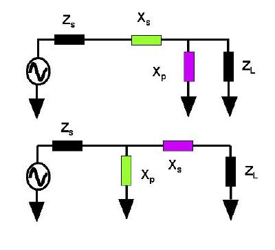
Usually Zs and ZL, the source and load
impedances to be matched, are not resistances (but they must
contain a finite resistive part). Just the same, the matching
reactances Xp and Xs (p for parallel and s
for series) are usually opposite in sign (hence the different
colours in the figure). i.e. if one is inductive the other is
capacitive. The choice between these configurations depends on
which of Zs or ZL is the greater. The
parallel or shunt element always appears across the impedance with
the higher (series) resistance.
To get an idea of how to employ Q to do such a design consider the
following example.
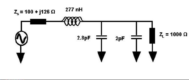
EXAMPLE
Suppose that Zs = 100 + j126 Ohms and ZL =
1000 Ohms in parallel with 2 pF. Design a matching network for 100 MHz.
Solution
A sensible choice in this case would be a circuit in the form of the
first above with Xs inductive (in this way it can absorb
the reactive part of Zs which is inductive) and
Xp capaciive so it can absorb the 2 pF. As a result we can
do the design for the 100 Ohm and the 1000 Ohm and forget about the
reactive parts of the source and load impedance which can be absorbed
into Xs and Xp later on.
It is easy to see what we are aiming to do. We will choose
Xp to divide down the 1000 Ohms to 100 Ohms (since shunting
a resistor with a reactance always reduces its value). Of course this
will also produce a reactive part which in this case will be
capacitive. The 2 pF will make it even more capacitive. So we then
choose Xs to cancel out both this combined capacitive
reactance and the inductive (+j126 Ohm) of the source impedance
Zs.
Exercise. What if the inductive part of Zs were too large to cancel?
The first trick is the following. If the resistance looking into the
shunt pair Xp and ZL has to be equal to the real
part of Zs (100 Ohm) and the reactances are equal and
opposite (viz equal complex conjugates have equal real parts and equal
and opposite imaginary parts), then the Q's of the elements made of
Zs, Xs and Zp, Xp must be
equal. Using the result derived in Q2, we may therefore write
Q = (1000/100 - 1)1/2 = 3.
A bit of a low value for some applications (but never mind we'll deal
with this in a minute. Here we have no choice). Given Q we can
immediately determine the magnitude of Xp from
Xp = 1000/Q = 333 Ohm hence Zp = -j333 Ohms. At
100 MHz this amounts to Cp = 4.8 pF. Since there is
already 2 pF shunting (-j796 W) the load we
only need Cp = 2.8 pF. Similarly Xs = Q*100 =
300 Ohms hence Zs = j300 Ohms. At 100 Mhz this is
Ls = 477 nH. Since j126 Ohm correeponds to 200 nH at 100
MHz, we only need Ls = 277 nH. We finally obtain the
following network...
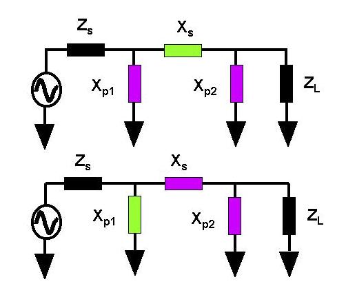
PI and T NETWORKS
In order to build higher Q networks (higher than the L-network Q) , PI
or T-section networks provide a solution. The following figure shows
the possible PI configurations. The colours are meant to indicate
possible opposite values in the sign of reactance.
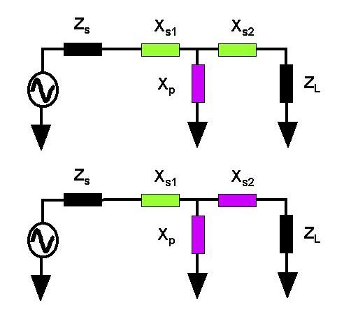
Below are the T-networks.
An obvious way to design a PI matching network is shown in the
following figure. In this trick, the PI network is decomposed into two
back to back L-networks whose Q can be chosen. A virtual resistance R
terminates each sub-network in the centre. The idea is that the left
circuit is coupled to the resistor R via an L network. The circuit at
the right is effectively fed from a circuit of source resistance R via
its own L network.
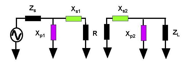
The virtual resistor is used to program the Q as follows,
Q = (Rmax/R - 1)1/2
where Rmax is the maximum of the load or source
resistors. R must be smaller than both the load or source resistors
because it is connected in a series arm and must have a low value to
produce a high Q. Notice that this is the result of Q2 again
because both L-networks have the property that R with
Re(Zs) on the left and R with Re(Zp) on the
right are in series shunt pairs.
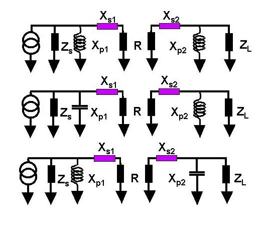
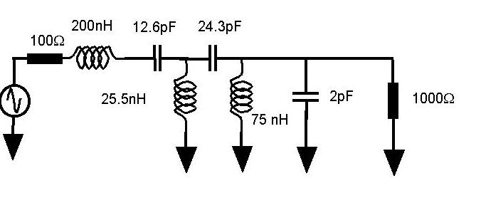
EXAMPLE
Consider again the case of the above example. Now design a PI matching
network with a Q of 20 that (unlike in the above example) can block
the flow of DC.
Solution
In principle, any one of the following circuits could do the job
keeping in mind that XS1 or XS2 or both must be
a capacitor in order to block the flow of DC.
The reactance values can all be determined in one fell swoop and we
can think about their signs later. Firstly, R = 1000/(1 +
Q2) = 2.5 W. Once again,
forgetting about the 2 pF and the +j126 W,
we can say that for the right circuit, Xp2 = 1000/20 = 50
and Xs2 = 20*2.5 = 50. The Q for the left circuit must be
given by Q = (Rs/R - 1)1/2 = (100/2.5 -
1)1/2 = 6.25. Therefore Xp1 = 100/6.25 = 16
and Xs1 = 6.25*2.5 = 15.6.
For the first circuit, Xp2 || 2 pF = j50 W . So Xp2 becomes j47.
Xs = -j65.6 W and Xp1
= 100/6.25 = j16W. To cancel the +j126
W, insert -j126 W (12.6 pF).
We obtain the following circuit.
Exercises
- Design a Q = 10 T-network for 30 MHz from a 10W source to a 50 W
load that can pass DC. Use MATLAB to compute the circuit's transfer
function and return loss around 30 MHz.
- Construct the above circuits in the example and the first exercise
and test then using the VNA.
|