Data sheets for both FET and Bipolar Junction RF power transistors
carry two essential pieces of information for RF power circuit design.
These are the large-signal equivalent input and output impedances and
the output power obtainable as a function of input power. The large
signal input and output impedances could either be in series or
parallel form but using the the
relations for these interms of circuit Q, it is easy to convert.
Take a look at Figures 2-8 and Figure 15 of the MRF134 data. These parameters are for high
power design and would have quite different values in the small signal
case. Notice that the S-parameters are also available in Table
1. These are only relevant for small signal operation and should only
be used for a first attempt at a high power design. By now we are good
at this.
Often the resistive part of the output impedance is not given. For
example, if one looks at page 2 of the MRF134 data, only the
capacitances are listed. These capacitances have the same meaning as
they did for the bipolar transistor and do allow an RF equivalent
circuit to be developed. For high power design we assume that the load
resistance that we require is that which gives our desired power for
the maximum possible excursion of the output voltage VIZ RL
= (VDS - Vsat)2/(2P). We therefore
must include a matching network to make that tunes out the capacitance
of the output stage and makes the load impedance (Z0 if
connecting to a transmission line) equal to this value.
Example
Since the design of RF transistor amplifers involves no new
concepts, we go through the design of the 150 MHz test circuit in the
MRF134 data sheet.
Consider the input circuit in Figure 1. We can summarise it as follows.
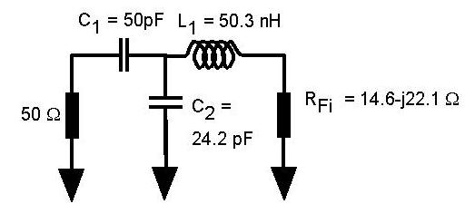
The 68 Ohm will be ignored in the following
because it says in Figure 15 of the data sheet that it was included in
the measurement of the input FET impedance = 14.6 - j22 Ohm. In doing this design we don't know in advance
what Q the design engineer had chosen. However the circuit indicates
considerable variability in component values to allow for variations
in the transistor parameters. By assuming C1 = 50 pF, we
can start the calculation. In retrospect we'll see that a Q of about
2 was intended. Of course in doing our own designs we would pick Q
first!
Using the technique described in the chapter on matching, we recognise
the matching circuit as a T-network. We therefore include a virtual
resistor as shown in the following.
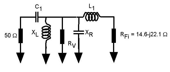
Note that capacitor C2 has been split into an L in the left
circuit and a C in the right circuit because of their respective
requirements for the achievement of a complex conjugate. Since
Rv is in a parallel combination (in both the left and the
right circuits), its value must be greater than the RS = 50
Ohm (source resistance) or RFi =
14.6 Ohm the FET input resistance. According
to our recipe for determining Q the larger Q would be given by Q =
QR = (Rv/RFi - 1)1/2, where
the R subscript refers to the right circuit. Similarly QL
= (Rv/RS - 1)1/2.
Consider the left circuit. Since we know C1 with
X1 = 21.2 Ohm at 150 MHz,
QL = X1/RS = 0.424. We obtain
Rv = RS(1 + .4242) = 59 Ohm. The part of C2 (which is an
inductor in the left circuit) is given by Rv/X2L
= .424 => X2L = 139Ohm.
Consider the right circuit. From the above expression for Q we obtain
QR = (Rv/RFi - 1)1/2 =
(59/14.6 - 1)1/2 = 1.74. The part of C2 (which
is a capacitor in the right circuit: To be checked ) is given by
Rv/X2R = 1.74 => X2R = 33.3 Ohm. The combined reactance of L2 and
the reactance of the FET, call it X1R' =
QRRFi = 1.74*14.6 = 25.4 Ohm. Thus L1 = (25.4 + 22.1)/(2p150MHz) = 50.3 nH.
Thus we are justified in using a capacitor for C2. If we
wish to replace the left and right shunt elements by a single
capacitor then we combine the j139Ohm and the
-j33.3Ohm in parallel, which corresponds to
C2 = 24.2 pF for operation at 150 MHz.
This completes the design of the input circuit.
The output circuit looks as follows.
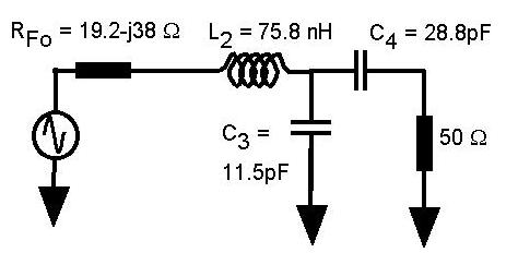
The procedure is similar to that for the input circuit. Here however
we may as well assume a Q of 1.74 so that the input and output Q's are
at least matched. In the case of the output circuit, we are
transforming from the output of the transistor to the 50 Ohm load, but this makes no difference. The virtual
resistor is given by Rv = RFo(1 + Q2)
= 77.3 Ohm where RFo = 19.2 Ohm is the FET output resistance. The final values
obtained are L2 = 75.8 nH, C3 = 11.5 pF and
C4 = 28.8 pF. Once again we have chosen to lump the left
and right circuit shunt reactances into C3 as required.
The inductor dimensions are given in the Caption for Figure 1. Using
the formula for inductance
with N = 3, r = .394cm and l = .51 cm for L1 in the
input circuit and N = 3.5, r = .394 cm and l = .635 cm for L2 in the
output circuit, we obtain, L1 = 63.7 nH and L2 =
75.7 nH.
You may try the following...