A good place to start is with the SR latch, and see how it can in principle be constructed using feedback and combinational elements.
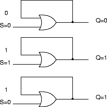
Figure 53 shows a set latch, i.e. a latch which can only be set.
When S is set to 1, this logical value is transferred to the output Q (after a non-zero propagation delay). The output is fed back to the input of the OR gate, so if S is now reset to 0, the gate remains set at 1. This latch can be set, but not reset.
Similarly, Figure 54 shows a reset latch, which can only be reset.
Describe for yourself the operation of this circuit.
In general we need a latch which can both be set and reset. We consider two designs.
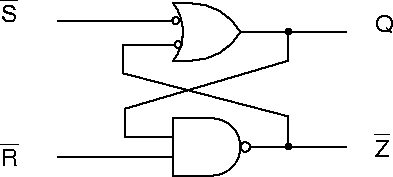
Figure 55 shows a NAND-based SR latch.
Note the double feedback. Like the latches above, this SR latch has two states:
| S | R | Qt+ | Zt+ | mode |
| 0 | 0 | Qt | Qt | HOLD |
| 0 | 1 | 0 | 0 | RESET |
| 1 | 0 | 1 | 1 | SET |
| 1 | 1 | 1 | 0 | AMBIGUOUS |
Here, Qt refers to the current state value, and Qt+ refers to the next state value.
In terms of equations,
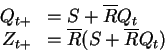
This circuit is set dominant, since S=R=1 implies Q=1.
Note that Q=Z except when S=R=1.
If we disallow the input combination S=R=1, then the outputs Q and Z are called mixed rail, meaning that they are logically identical but are of opposite activation level.
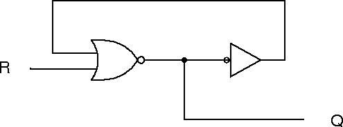
So if we adopt the convention of disallowing S=R=1, we can draw the NAND-based SR latch as in Figure 56.
The state transition table for the NAND-based SR latch is as follows:
|
|
S | R |
| 0 | ||
| 1 | ||
| 0 | 1 | |
| 1 | ||
| 0 |
State transition tables are useful for state machine synthesis. The right two columns tell you the inputs required to effect the state transition in the right column.
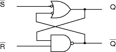
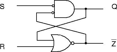
Figure 57 shows a NOR-based SR latch.
The NOR-based SR latch is reset dominant, as can be seen from its operation table:
| S | R | Qt+ | Zt+ | mode |
| 0 | 0 | Qt | Qt | HOLD |
| 0 | 1 | 0 | 0 | RESET |
| 1 | 0 | 1 | 1 | SET |
| 1 | 1 | 0 | 1 | AMBIGUOUS |
In terms of equations,
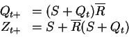
This the outputs Q and Z are also mixed rail if we exclude the input combination S=R=1.
The state transition table for the NOR-based SR latch is:
|
|
S | R |
| 0 | ||
| 1 | ||
| 1 | 0 | |
| 1 | ||
| 0 |
In summary, we see that an SR latch can be implemented in two ways, using either NAND gates or NOR gates.
The basic features of the SR latch (independent of implementation) are as follows.
Operation table:
| S | R | Qt+ | mode |
| 0 | 0 | Qt | HOLD |
| 0 | 1 | 0 | RESET |
| 1 | 0 | 1 | SET |
| 1 | 1 | - | INVALID |
|
|
S | R |
| 0 | ||
| 1 | 0 | |
| 0 | 1 | |
| 0 |
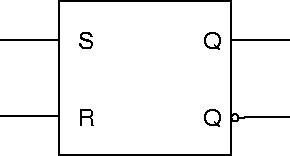
The standard circuit symbol for the SR latch is given in Figure 58.
ANU Engineering - ENGN3213