[ENGN2211 Home]
As an example of a FET amplifier, consider the JFET amplifier
of Figure 136.
Figure 136:
n-channel JFET small signal common source amplifier.
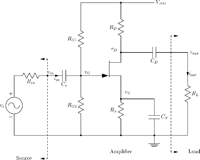 |
The JFET has parameters
IDSS=11 mA, Vp = -2 V.
We will use the component values RD = 1.2 k ,
RS=680 ,
RG1=5 M,
RG2=470 k,
VDD=30 V.
,
RS=680 ,
RG1=5 M,
RG2=470 k,
VDD=30 V.
The voltage divider bias network gives
and since IG =0 we get
VG = 2.58 V.
Now
VS = ID RS
and so
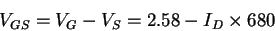 |
(128) |
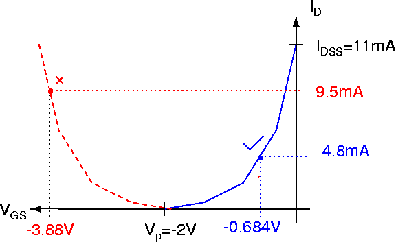
The square law (110) gives
and solving this for ID gives two
solutions 4.8 and 9.5 mA. The smaller value
is the correct one since the larger one is in a region
where the quadratic formula is not a valid model.
Why is this? Take a look at Figure 137
(the values of VGS can be found using equation (128).
Figure 137:
Square law and correct bias point determination.
 |
Therefore
Next,
VDD = ID RD + VDS + ID RS
and so
This determines the DC operating point Q.
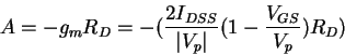
Now let's calculate the voltage gain
neglecting the influence of the source and load resistance.
The source resistor RS is short-circuited to AC signals by
the bypass capacitor CS, so the AC equivalent circuit is
as in Figure 138.
Figure 138:
AC equivalent circuit.
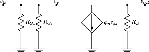 |
Now
vgs=vin, and
vout = - (gm vgs)RD = - gm RD vin .
Therefore
and so
A = -8.7.
It is straighforward to check that the input resistance
is given by
and the output resistance is
rout = RD .
Exercise.
Find the gain from vs to vout including the effects of source and load
resistances.
[ENGN2211 Home]
ANU Engineering - ENGN2211