The following design tasks are to be performed
before coming into the laboratory. Do all work in your notebooks.
a.
Draw truth tables (Table 20) for the
two modules PLUS and MINUS, making use of doesn't matter inputs
and don't care outputs. To do this,
consider
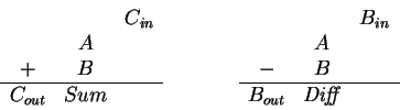
Here, Cin is the incoming carry bit, Cout is the
outgoing carry bit,
Bin is the incoming borrow bit, and Bout is the
outgoing borrow bit.
Table 20:
Design logical truth tables.
Cin
A
B
Sum
Cout
0
0
0
0
0
1
0
1
0
0
1
1
1
0
0
1
0
1
1
1
0
1
1
1
Bin
A
B
Diff
Bout
0
0
0
0
0
1
0
1
0
0
1
1
1
0
0
1
0
1
1
1
0
1
1
1
b.
Find simple Boolean expressions for Sum, Cout,
Diff and Bout.
Use of K-maps is recommended.
c.
Design a circuit using TTL gates.
You may use mixed logic. Assume all inputs and outputs are
ACTIVE HIGH. Parts should be drawn from those available
in the Digital Design Lab (see web page for a list of available parts).
d.
Using PSPICE, simulate your circuit and
verify the correct operation of your design,
Table 21.
Include a printout from PSpice of your circuit in your notebook.