


[ENGN2211 Home]
Small Signal Amplifier
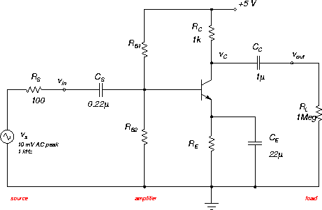
Load the PSPICE file
bjt-amp1.sch,
Figure 37.
Your task is to design values of RB1, RB2
and RE for good gain and input level.
Figure 37:
Small signal amplifier.
 |
Exercise:
- 1.
- Using the relations
select (standard) values of RB1 and RB2
so that
 V,
V,
 k
k (as in the previous bias section).
Set these values in PSPICE.
(as in the previous bias section).
Set these values in PSPICE.
- 2.
- Now choose RE so
 mA (for maximum possible
AC swing). Set in PSPICE.
mA (for maximum possible
AC swing). Set in PSPICE.
You may use your curves from the DC bias exercise above, section 7.4,
to find RE.
- 3.
- Simulate and check that your DC bias point is correct.
Record your values.
Draw the load line on the characteristic graph (IC vs VCE) for your value of
RE.
Plot the DC operating point Q on this load line.
Check for consistency with the DC bias exercise above, section 7.4.
- 4.
- Enable transient analysis and simulate. Observe the input
and output waveforms. What is the voltage gain from the source voltage vs to the output load
voltage vout (As,out)?
Compare with theory.
Lecture Notes : BJT Transistor Circuits : Small Signal Amplifier : AC Analysis
To measure the gain, measure the peak-to-peak values of vs and vout
and calculate the ratio
vout/vs.
- 5.
- Repeat the transient simulation for increasing magnitudes
of the source voltage vs, and determine the maximum magnitude
of the input signal before the output waveform is clipped.
Note any distortion.
- 6.
- Set the magnitude of vs back to its original value,
and now vary the source RS (increase it) and load RL (decrease it)
resistances (individually).
Note the influence on gain. Discuss.
[ENGN2211 Home]
ANU Engineering - ENGN2211