next up previous contents

[ENGN2211 Home]

   
DC Bias

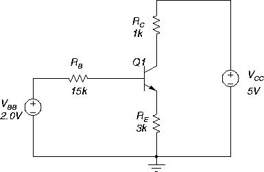
Load the PSPICE file bjt-dc3.sch, Figure 35. This circuit will have the same DC bias as the amplifier circuit of section 7.5.

Lecture Notes : BJT Transistor Circuits : DC Bias


Figure 35: Circuit for BJT DC operating point.
\begin{figure}
\begin{center}
\epsfig{file=images/clab6img5.eps}\end{center}\end{figure}

Exercise:

1.
Simulate the circuit for the given setup. Is the transistor Q1 in the active mode? Why?
It may be helpful to refer to the transistor characteritics obtained earlier (it is the same transistor).

2.
We now wish to investigate the effect of varying the emitter resistor RE on the DC operating point, and in particular on IC and VCE. We do this using DC sweep, with RE set up as a parameter, varying between 100 $\Omega$ and 5 k$\Omega$.

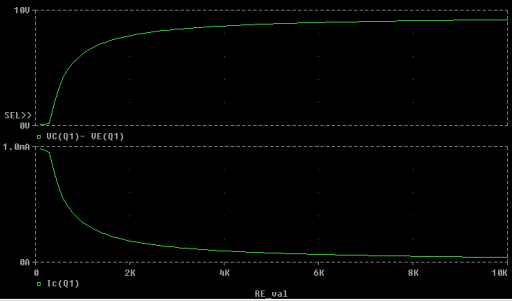
Enable DC sweep and simulate again. Obtain plots of IC and VCE vs RE, (something like Figure 36). (Recall that VCE=VC-VE!)

3.
Explain what you see.
Note carefully the effect of RE on IC and VCE.

4.
Draw load lines on the characteristic graphs (IC vs VCE) for three values of RE: 0.5, 1.0 and 3.0 k$\Omega$.
The horizontal intercept is VCC=5 V, and the vertical intercepts are given by

\begin{displaymath}I_{C(sat)} = \frac{V_{CC}}{R_C+R_E}
\end{displaymath}

Plot the operating point Q corresponding to item 1 (on the RE=3 k$\Omega$ load line).


Figure 36: DC operating point varies with RE.
\begin{figure}
\begin{center}
\epsfig{file=images/clab6img6.eps}\end{center}\end{figure}


next up previous contents

[ENGN2211 Home]

ANU Engineering - ENGN2211