


[ENGN3213 Home]
To view the schematic diagram of the digital circuit,
click on the right-most symbol in the Design Entry icon.
The Schematic Editor window will appear.
Open the andor.sch schematic
File  Open...
and the circuit diagram will appear
Figure 8 (you may need
to scrol to locate it in the bottom right corner).
Figure 8:
Schematic editor showing diagram andor.sch.
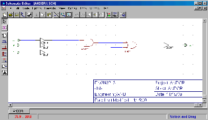 |
Notice:
- 1.
- The title block in the bottom right of the page.
It contains helpful labeling and and other information.
It can be edited using File Table Setup...
Replace the contents of line 3 with your name and student number.
Always put your name and student number in all of your
diagrams and source files.
- 2.
- The two gates AND and OR are shown.
- 3.
- The inputs A, B, C, are shown with labeled terminals,
and these are connected to IBUF components. The IBUF components
are used to tell the software that these terminals are to be connected
to the outside world via pins on the FPGA chip for input.
- 4.
- The output X is shown with a labeled terminal,
and this is connected to an OBUF component. The OBUF component
is used to tell the software that these terminals are to be connected
to the outside world via pins on the FPGA chip for output.
- 5.
- It is possible to specify the pin locations on the schematic
diagram. Instead, it is often more convenient
to do this in a separate file, andor.ucf.
To view this file, use the HDL Editor.
In the main window, click on the left-most HDL symbol
on the Design Entry icon, and when the editor window
opens select Existing document
and open andor.ucf. You will see the following text:
NET A LOC=P19;
NET B LOC=P20;
NET C LOC=P23;
NET X LOC=P61;
This information maps A to pin number 19 on the Xilinx chip, etc,
as will be explained further in HLAB1.
[ENGN3213 Home]
ANU Engineering - ENGN3213