


[ENGN3213 Home]
So far we have created the lowest level in our design, the 1-bit
full adder. The complete 4-bit adder will be created using
hierachical design, widley used in digital systems design.
This is similar to the use of subroutines in computer programming.
We will create a macro symbol from the full adder schematic,
and then include this in a top-level schematic.
To create the macro symbol:
- 1.
- If necessary, re-open the full adder schematic adder-s1.sch
in the Schematic Editor.
- 2.
- Create the macro symbol as follows
Hierachy  Create Macro Symbol From Current Sheet
The symbol name should be adder-s1.
Make sure the inputs and outputs are correct.
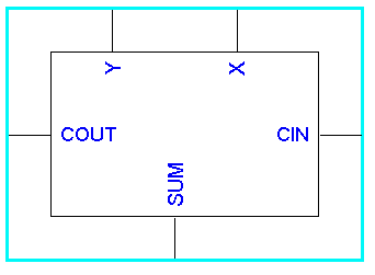
The symbol should now be created. We will edit it's shape
using the Symbol Editor:
- 1.
- From the Schematic Editor window,
Tools Symbol Editor
and select the symbol adder-s1.
- 2.
- In the Symbol Editor, using the mouse to drag the inputs and outputs,
rearrange the symbol so it has the appearance shown in Figure 18.
- 3.
- Save, and quite the Symbol Editor.
Figure 18:
Full adder symbol.
 |
The top level schematic file adder4-s.sch is contained
in the ZIP file
adder4-s.zip.
Download this file and extract it into your
main project directory adder4-s.
- 1.
- In the Schematics Editor, open the top level file
adder4-s.sch.
- 2.
- Add this sheet to the project.
(Use the method above Hierachy Add Sheet to Project,
or alternatively, in the Project Manager window,
use Project Add Source Files... and select adder4-s.sch.
- 3.
- You will see that this schematic is incomplete, since the full adder module
has not been included. Open the Symbol toolbox, and note that
the macro symbol adder-s1 appears in the parts list,
Figure 19.
- 4.
- Find the four locations for the full adders.
Carefully add four instances of adder-s1 to these locations,
Figure 20.
- 5.
- Since the connections might not match, as in Figure 20,
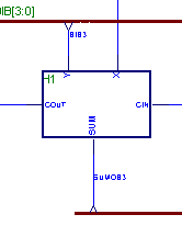
very carefully use the Select and drag mode to move the wires into place,
Figure 21.
Move the exact end of the wires into place; the solid dot should dissappear
indicating correct connection.
- 6.
- Save the edited file.
- 7.
- Create the netlist Options Create Netlist. Check the main
log window to check for any hanging wires. If there are any,
re-edit the schematic and remove these errors.
Figure 19:
Full adder symbol in the parts list.
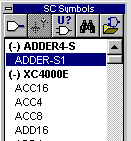 |
Figure 20:
Full adder symbol placed in top-level schematic (mis-matched wiring).
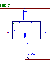 |
Figure 21:
Full adder symbol placed in top-level schematic (no mis-match).
 |
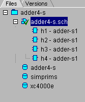
Upon successful completion, the project information should
appear as in Figure 22. The four
full adder components are listed.
Figure 22:
Complete adder4-s project.
 |
Notes:
- 1.
- The solid lines in the top-level schematic adder-4s.sch
are buses. These were inserted using the draw buses mode.
The buses were named differently to the external signal names
(see below).
- 2.
- Connections from the buses to the various components were made
using the Draw bus taps mode.
Note their naming.
- 3.
- Double clicking on wires/buses alows you to edit names.
- 4.
- The inputs
A3,A2,A1,A0,
B3,B2,B1,B0 and CIN, and outputs
SUM3, SUM2, SUM1, SUM0 and COUT are made available to the outside world
using IBUF and OBUF parts, and terminators.
[ENGN3213 Home]
ANU Engineering - ENGN3213