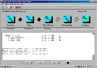
Next, implement the design for the Xilinx hardware (4003EPC84 chip). Click on the implementation icon, check that the correct device has been selected (should be OK), select RUN, and watch the implementation process, Figure 10.
At the successful completion of the implementation process, you will be left with a .BIT file, andor.bit, which you will later download onto the hardware chip (HLAB1).
Note: Successful completion is indicated by a tick (check) on the implementation icon, and the programming icon becomes active. Sometimes this may not occur, in which case simply click on the implementation icon again, select NO, and then the download icon should become active.
ANU Engineering - ENGN3213