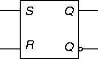
Latches are basic memory elements, Figure 42.
Data can be set Q=1 by setting S=1, or cleared Q=0 by setting R=1, or stored by setting S=R=0. Latches are not clocked. Here is the truth table for the SR latch:
| S | R | Q+ | function |
| 0 | 0 | Q- | store |
| 0 | 1 | 0 | reset |
| 1 | 0 | 1 | set |
| 1 | 1 | - | - |
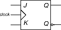
Flip flops are the basic memory element in a clocked circuits. They are essentially latches which are permitted to change state only at times determined by a clock signal, Figure 43.
Here is the truth table for the JK flip flop:
| J | K | Q+ | function |
| 0 | 0 | Q- | store |
| 0 | 1 | 0 | reset |
| 1 | 0 | 1 | set |
| 1 | 1 |
|
invert |
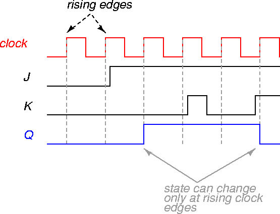
A rising edge triggered JK flip flop is only permitted to change state at the time of the rising edge of the clock signal, Figure 44.
ANU Engineering - ENGN3213