Historically the TTL series has been very important and widely used, but is now being taken over by CMOS. TTL is high speed, low power, and economical.
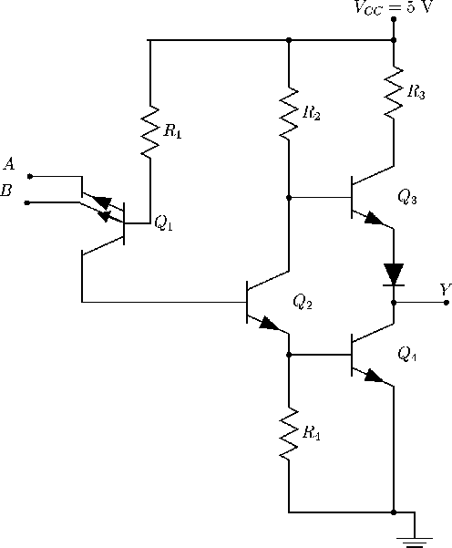
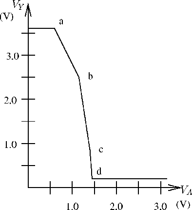
A standard TTL NAND gate is shown in Figure 3, with transfer characteristic shown in Figure 4.
Acceptable values for L might be 0-0.8 V, and for H, say 2.0-5.0 V. Detailed information on the voltage values can be found in the TTL data sheets. Propagation delay for 74LS devices is 9.5 ns, and fan-out is 20. Noise margin is of the order 400 mV.
In Figure 3, the transistor Q1 is called a multiple-emitter transistor. The transistors Q3 and Q4 form an output arrangement called totem-pole. Transistor Q3 provides an active pull-up output (instead of a passive resistor), which is fast.
If A or B is L, then Q1 and Q3 are on, and Q2 and Q4 are off, so that Y is H. In fact Y will be around 3.4-3.8 V. If a load is connected to Y, increased current will be drawn through resistor R3 causing the collector voltage of Q3 to fall, and if the load current is too great (say caused by a number of load gates greater than the fan-out) then the logic level at Y may be invalid. A substantial current IIL of the order 1.1 mA will flow out of the input A, and so the input source acts as a sink to ground for this current.
If both A and B are H, then Q1 and Q3 are off, and Q2 and Q4 are on,
so Y is L, around 0.2 V. With Q3 off, the main source off current through
Q4 is from the output Y (which is typically connected to other TTL inputs).
The output impedance when Q4 is on is low, typically 10 ![]() .
Only a small current IIH of the
order 10
.
Only a small current IIH of the
order 10 ![]() A needs to be supplied from the input source.
A needs to be supplied from the input source.
The truth table which summarises the behaviour of this NAND gate is
| INPUT | OUTPUT | |
| L | L | H |
| L | H | H |
| H | L | H |
| H | H | L |
Other types of physical gates are availables, such as NOR, etc.
ANU Engineering - ENGN3213