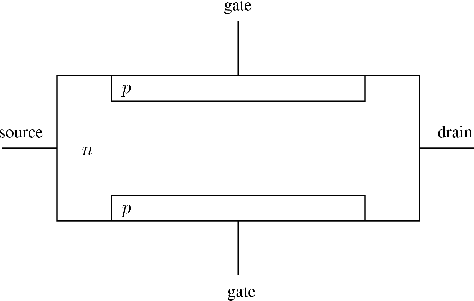
A schematic representation of an n channel JFET is shown in Figure 118. An n-type channel is formed between two p-type layers which are connected to the gate. Majority carrier electrons flow from the source and exit the drain, forming the drain current. The pn junction is reverse biased during normal operation, and this widens the depletion layers which extend into the n channel only (since the doping of the p regions is much larger than that of the n channel). As the depletion layers widen, the channel narrows, restricting current flow.
When
![]() ,
there is little voltage drop
along the length of the channel, and the depletion regions are parallel,
Figure 119. As vGS is increased negatively,
they eventually touch reducing iD to zero. The value of vGS
at which this occurs is called the pinch-off voltage, Vp
(or
vGS(off)).
,
there is little voltage drop
along the length of the channel, and the depletion regions are parallel,
Figure 119. As vGS is increased negatively,
they eventually touch reducing iD to zero. The value of vGS
at which this occurs is called the pinch-off voltage, Vp
(or
vGS(off)).
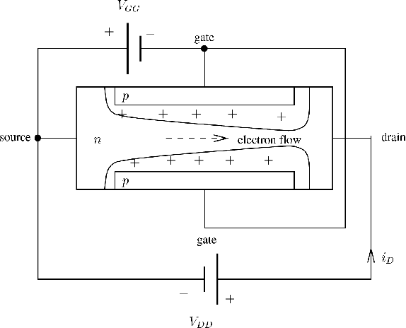
When
![]() ,
there is a voltage drop
along the length of the channel, and the depletion regions are no longer
parallel, but are closer together towards the drain, Figure 120.
As vDS is increased, they will touch (pinch-off) towards the drain, and the
drain current iD can increase no longer. At the threshold of pinch-off,
vGS-vDS=Vp.
As vDS is further increased, iD remains constant, and the JFET is
in its current saturation region, the normal mode of operation.
(This constant current region is a characteristic feature of
any transistor, FET or BJT.)
The channel shape remains unchanged, with a small region of touch near
the drain, and further increases in vDS occurs across this small region.
,
there is a voltage drop
along the length of the channel, and the depletion regions are no longer
parallel, but are closer together towards the drain, Figure 120.
As vDS is increased, they will touch (pinch-off) towards the drain, and the
drain current iD can increase no longer. At the threshold of pinch-off,
vGS-vDS=Vp.
As vDS is further increased, iD remains constant, and the JFET is
in its current saturation region, the normal mode of operation.
(This constant current region is a characteristic feature of
any transistor, FET or BJT.)
The channel shape remains unchanged, with a small region of touch near
the drain, and further increases in vDS occurs across this small region.
JFETS are high input impedance devices, and so
![]() (due
to the reverse bias pn junctions).
(due
to the reverse bias pn junctions).
ANU Engineering - ENGN2211