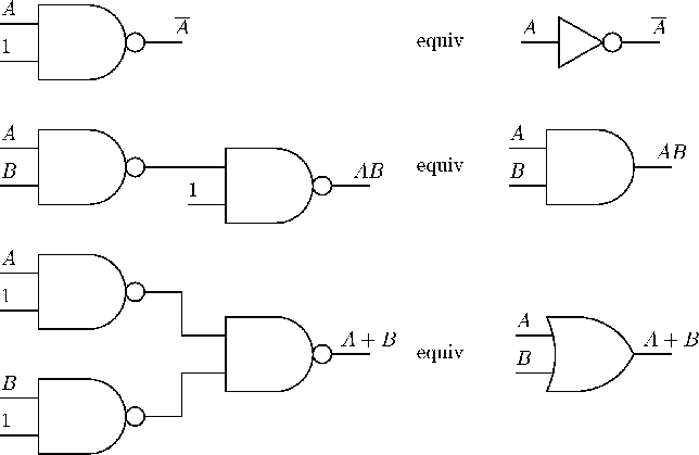
We know that all boolean functions can be expressed in terms of AND, OR and NOT. In fact, all boolean functions can be expressed in terms of either
To see this, let's show that NAND gates can be used to implement
NOT, AND and OR.
Algebraically, we have
Exercise. Using Boolean algebra, show how to obtain A+B from NAND gates.
The universality of NAND is illustrated in Figure 157.
Exercise. Show how NOR gates can be used to implement AND, OR, and NOT.
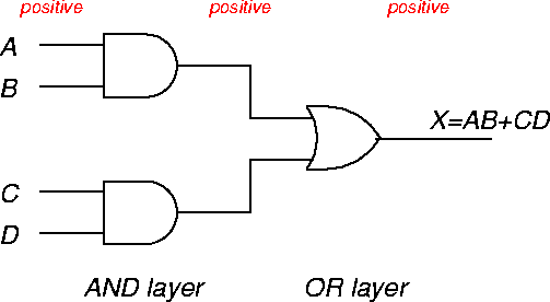
Example.
Implement the logic function
We first implement as using AND and OR as shown in Figure 158.
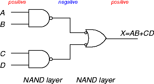
This implementation requires two ICs. Next, we draw bubbles as shown in Figure 159.
The AND level clearly becomes a NAND level. But by De Morgan, the OR gate has become also a NAND gate. Between the two levels, we are using negative logic, and the bubbles are used to denote this. At the input side and also at the output side, we are using positive logic, and the absence of bubbles indicates this. So the circuit of Figure 159 is interpreted in mixed logic. This NAND gate implementation requires only one 74LS00 chip.
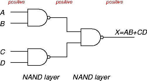
The circuit of Figure 159 is identical to Figure 160, where we have explicitly drawn the second level NAND gate in positive logic form. This circuit is interpreted purely in positive logic, and the bubbles denote inversion. However, this circuit is harder to read than Figure 159.
So mixed logic can be helpful for implementation and for interpreting logic circuit diagrams.
ANU Engineering - ENGN2211