next up previous contents index

[ENGN2211 Home]

Boolean Functions

NOT.  

\begin{displaymath}\overline{A} = \ {\rm NOT} \ A
\end{displaymath}

So $\overline{A}$ is the complement of A, defined by the truth table  
A $\overline{A}$
0 1
1 0

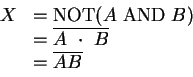
A truth table defines the boolean function by specifying the boolean output value associated with each boolean input value.

The circuit symbol for the NOT function is the inverter, Figure 148.   The bubble denotes inversion (complement).


Figure 148: NOT gate.
\begin{figure}
\begin{center}
\epsfig{file=images/diglogimg1.eps}\end{center}\end{figure}

Interestingly, in Quantum Computing there is a $\sqrt{{\rm NOT}}$ gate, but that is another story.
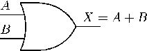
OR.  

\begin{displaymath}\begin{array}{rl}
X & = A \ \mbox{{\sc OR}} \ B \\
& = A \ + \ B
\end{array}\end{displaymath}

Here + denotes OR, defined by:
A B X=A+B
0 0 0
0 1 1
1 0 1
1 1 1

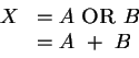
OR is like two switches A, B is parallel; one or both open lets current flow. The circuit symbol is shown in Figure 149.
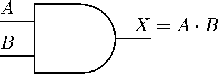

  
Figure 149: OR gate.
\begin{figure}
\begin{center}
\epsfig{file=images/diglogimg2.eps}\end{center}\end{figure}

AND.  

\begin{displaymath}\begin{array}{rl}
X & = A \ \mbox{{\sc AND}} \ B \\
& = A \ \cdot \ B \\
& = AB
\end{array}\end{displaymath}

Here $\cdot$ denotes AND, defined by:
A B $X=A\cdot B$
0 0 0
0 1 0
1 0 0
1 1 1

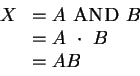
AND is like two switches A, B is series; both must be open for current to flow. The circuit symbol is shown in Figure 150.


Figure 150: AND gate.
\begin{figure}
\begin{center}
\epsfig{file=images/diglogimg3.eps}\end{center}\end{figure}

These three are the most basic logic functions, and define the Boolean algebra on the set ${\cal B}$.

Also important are the following functions.
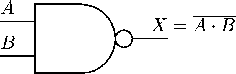
NAND.  

\begin{displaymath}\begin{array}{rl}
X & = {\rm NOT} (A \ \mbox{{\rm AND}} \ B) \\
& = \overline{A \ \cdot \ B} \\
& = \overline{AB}
\end{array}\end{displaymath}

NAND is defined by:
A B $X=\overline{AB}$
0 0 1
0 1 1
1 0 1
1 1 0

NAND is the complement of AND. The circuit symbol is shown in Figure 151. (We encountered the physical NAND gate in section 10.3.)
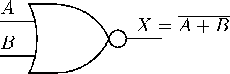

  
Figure 151: NAND gate.
\begin{figure}
\begin{center}
\epsfig{file=images/diglogimg4.eps}\end{center}\end{figure}

NOR.  

\begin{displaymath}\begin{array}{rl}
X & = {\rm NOT} (A \ \mbox{{\rm OR}} \ B) \\
& = \overline{A \ + \ B} \\
\end{array}\end{displaymath}

NOR is defined by:
A B $X=\overline{A+B}$
0 0 1
0 1 0
1 0 0
1 1 0

NOR is the complement of OR. The circuit symbol is shown in Figure 152.


Figure 152: NOR gate.
\begin{figure}
\begin{center}
\epsfig{file=images/diglogimg5.eps}\end{center}\end{figure}

NAND and NOR are very important building blocks.

XOR.  

\begin{displaymath}\begin{array}{rl}
X & = A \oplus B \\
& = \overline{A} B + A \overline{B}
\end{array}\end{displaymath}

XOR is defined by:
A B $X=A \oplus B$
0 0 0
0 1 1
1 0 1
1 1 0

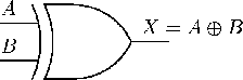
XOR is true if one and only one of A, B is true; hence the term exclusive OR.  . The circuit symbol is shown in Figure 153.


Figure 153: XOR gate.
\begin{figure}
\begin{center}
\epsfig{file=images/diglogimg6.eps}\end{center}\end{figure}

XOR is useful in

EQV.  

\begin{displaymath}\begin{array}{rl}
X & = A \odot B \\
& = \overline{A} . \overline{B} + A B
\end{array}\end{displaymath}

EQV is defined by:
A B $X=A \odot B$
0 0 1
0 1 0
1 0 0
1 1 1

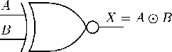
EQV is true only if both A and B are the same, and so is the complement of XOR. It is called equivalence or exclusive NOR.   The circuit symbol is shown in Figure 154.


Figure 154: EQV gate.
\begin{figure}
\begin{center}
\epsfig{file=images/diglogimg7.eps}\end{center}\end{figure}

EQV is useful for detecting equality.


next up previous contents index

[ENGN2211 Home]

ANU Engineering - ENGN2211