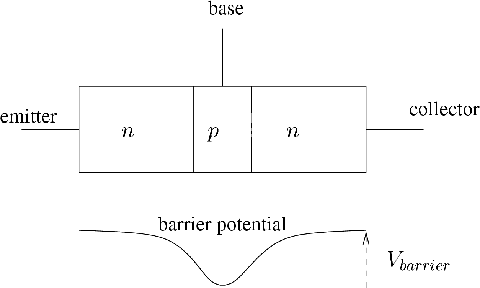
The npn transistor consists of a thin, lightly-doped p-type layer sandwiched between two n-type regions, Figure 93.
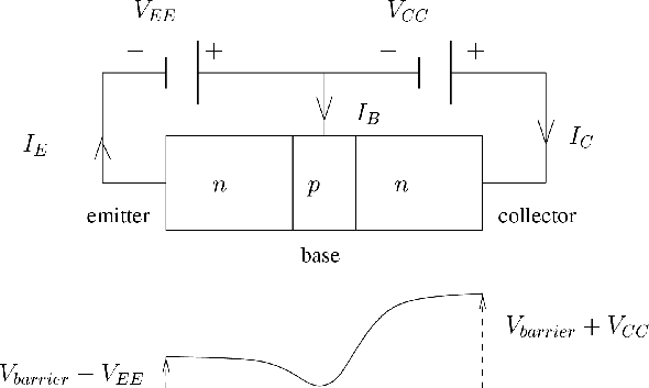
In normal operation under normal bias conditions, the emitter-base junction is forward biased ( vBE > 0), and the collector-base junction is reverse biased ( vCB > 0), Figure 94 and Figure 95.
The voltages VBB and VCC indicate the voltages applied to achieve the forward EB and reverse BC biases. The EB depletion layer is narrowed, and the BC depletion layer is widened.
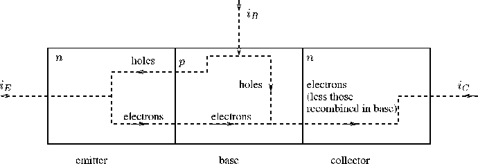
The n-type emitter region is heavily doped, and has a great many conduction band electrons which easily diffuse into the p-type base region. In the emitter the electrons are majority carriers while in the base they are minority carriers. The base region is thin and lightly doped, and so only a small fraction of the electrons injected into the base get recombined. The base current is small as a result. Most of the electrons get pulled into the n-type collector region by the reverse bias voltage, and form the collector current.
ANU Engineering - ENGN2211