Load the PSPICE file cmos-inv.sch, Figure 50.
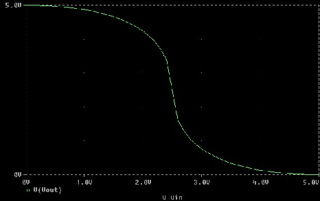
Simulate the circuit and obtain the INVERTER input-output curve of Figure 51. Explain, as best you can, what happens as Vin is increased from 0 V to VDD=5 V.
For Vin=0 V (i.e. LOW), work out the state or mode of operation for each transistor (on or off is OK), and deduce that Vout should be HIGH (value?)Do the same for Vin=5 V (i.e. HIGH), and this time deduce that Vout should be LOW (value?)
To do this, examine transistor currents and voltages.
ANU Engineering - ENGN2211