


[ENGN3213 Home]
It is recommended that the first thing you do in the lab is to get
a serial channel working. You are given some coldfire
and VHDL code to help (Appendix 17.8).
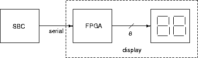
Figure 55 shows the
channel architecture. The Appendix 17.7
lists the MCF5206 serial channel 1 (uart1) registers.
Figure 55:
A one-way serial channel from the SBC to the FPGA/7-segment display.
 |
- 1.
- Using the code provided in Appendix 17.8,
implement
the one-way serial
channel. Your system should be capable of sending a pair of characters
(represented as one byte, i.e. 8-bits) from a data register in the SBC
to the display, using the FPGA as a receiver and other possible hardware functions
(such as decoding). Use 1200 baud.
- 2.
- Use the clock on the Digital Trainer Board to generate the clock signal
of the correct frequency for the FPGA serial receiver (see Appendix 17.8.2).
- 3.
- Program the SBC and FPGA and test your system. As part of the tests
use the CRO in one-shot mode to catch the serial packet.
Sketch the waveforms and check for correctness of the packet,
timing, etc. See Appendix 17.8.2.
[ENGN3213 Home]
ANU Engineering - ENGN3213