


[ENGN3213 Home]
- 1.
- The reaction timer will have a READY/RESET pushbutton (debounced).
In one state
the system is reset. When reset, upon activation of READY/RESET
the system will initiate
the reaction testing process. On completion of the testing process
(either normally with the time display, or abnormally with CHEAT
status), activation of READY/RESET causes the system to return
to the reset state.
- 2.
- At a random time between 1 and 9 seconds after READY is asserted,
the GO! led is asserted, signaling the start of the reaction timing.
The random time before the assertion of GO! removes the possibility of
anticipating the start of the timing period.
- 3.
- A pushbutton STOP switch is depressed to end the reaction time measurement
by stopping the timing process.
- 4.
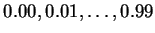
- The reaction time tr (0.XY seconds) is displayed by two 7-segment displays.
The error should be less than
 seconds, and the reaction time
is timed up to a maximum of tr = 0.99 seconds (a reaction time of
more than 0.99 seconds will be displayed as 0.99 seconds and the timing
process halted).
seconds, and the reaction time
is timed up to a maximum of tr = 0.99 seconds (a reaction time of
more than 0.99 seconds will be displayed as 0.99 seconds and the timing
process halted).
- 5.
- If the STOP button is depressed before the GO! led is asserted,
a CHEAT led should be asserted and the testing process halted.
- 6.
- The 7-segment displays
should be blanked until a valid measurement is complete.
A block diagram of the reaction timer is shown in
Figure 52.1
Your task is to design the circuitry for each module shown,
using the systematic design methods you have learned in
this course. In particular, you are to design the FSM controller
which controls the overall operation.
Figure 52:
Reaction timer block diagram.
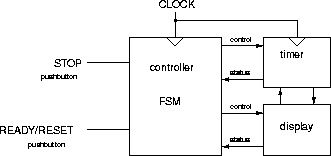 |
The following notes describe the function of each module
and give suggestions for implementation.
-
Controller FSM. The controller is to be a synchronous sequential
FSM. The clock frequency is 1kHz.
It receives input signals (debounced) READY/RESET and STOP,
signals from other modules, and issues signals to other modules.
Also, the controller should
automatically reset on power-up (SANITY).
-
Timer. The timer generates the random time interval of between
1 and 9 seconds and is responsible for reaction time measurement.
This later requirement involves a count sequence
 seconds.
It is a synchronous sequential machine.
seconds.
It is a synchronous sequential machine.
-
Display. The display module consists of two 7-segment displays for
displaying the reaction time,
and two leds for GO! and
CHEAT. The display should be blanked on reset.
The two pushbuttons on the digital trainer board are debounced.
[ENGN3213 Home]
ANU Engineering - ENGN3213