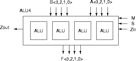
In this HLAB you are asked to implement and test on the Xilinx FPGA hardware a 4-bit ALU, Figure 45.
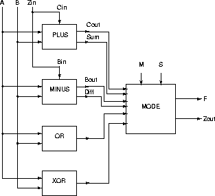
The table below describes the logical (M=0) and arithmetic (M=1) operations of a simple 1-bit ALU. The block diagram is shown in Figure 45.
| M | S | F |
| 0 | 0 | A + B |
| 0 | 1 |
|
| 1 | 0 |
|
| 1 | 1 |
|
The 4-bit ALU has 5 inputs
M,S,Zin,A,B and
two outputs F,Zout.
In logical mode, F is either A+B or
![]() depending
on the value of the selection bit S.
In arithmetic mode,
F, Zout is either the full adder output
or the full subtractor output of
A,B,Zin depending on the
value of the selection bit S (
Zin=Cin or Bin,
and
Zout=Cout or Bout).
depending
on the value of the selection bit S.
In arithmetic mode,
F, Zout is either the full adder output
or the full subtractor output of
A,B,Zin depending on the
value of the selection bit S (
Zin=Cin or Bin,
and
Zout=Cout or Bout).
ANU Engineering - ENGN3213