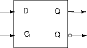
A gated D-latch, Figure 34, is a sequential module specified by the following table:
| G | D | Qt+ |
| 0 | 0 | Qt |
| 0 | 1 | Qt |
| 1 | 0 | 0 |
| 1 | 1 | 1 |
Note that the state Q is saved when G=0, and when G=1 we have Q=D. Thus the gated D-latch acts as a simple 1-bit memory element, with two states Q=0 and Q=1. It is an asynchronous module (no clock).
Create a new Xilinx schematic project called dlatch-s, download the zip file dlatch-s.zip and extract the schematic dlatch-s1.sch into your main project folder dlatch-s. Open the schematic and add to the project. Start the Logic Simulator.
ANU Engineering - ENGN3213