A traditional method for designing and building digital systems was to draw digital circuits on schematic diagrams and then to implement the circuits using, say, TTL or other standard digital ICs and gates such as AND, OR, MPX, etc. You did this in ENGN2211 and possibly elsewhere. CAD software tools for drawing and simulating digital schematics such as XILINX FOUNDATION are very useful and widely used. In place of discrete logic ICs, Programmable Logic Devices (PLDs) have come into widespread use, and include the Xilinx Field Programmable Gate Arrays (FPGA) devices used in this course. In this CLAB we will learn how to create combinational logic designs using schematic diagrams, simulate them, and compile them for FPGA implementation (in the hardware lab). In later CLABs and HLABs, we will use the VHDL Hardware Description Languages (HDLs) for describing digital circuits.
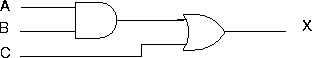
As an introductory example, we will use the combinational digital circuit of Figure 1.
This circuit represents the Boolean function
ANU Engineering - ENGN3213