The following material is largely based on the chapter on filter design in the book by Bowick. The procedure for designing filters is a predominantly prescriptive one. Nonetheless the techniques presented here are just scratching the surface of the subject of filter design. In the project, there is the design and implementation of a band pass filter to cover a chosen ISM band in the range 27 - 54 MHz. This is a very important part of the project because it is the role of the filter to reduce the bandwidth of unwanted signals intercepted by the antenna and to prevent the unwanted radiation of the harmonics of the power amplifier.
Specifying Filters
A filter is a two port device which passes a certain band of frequencies and attenuates others. The following parameters are therefore of interest.
The 3 dB limiting frequencies. For example for a low pass filter the upper 3 dB frequency is required. (3 dB frequency is the frequency at which the filter attenuates half the power of the input signal).
-
The degree of attenuation of out of band signals. This usually increases the further the frequencies of the signals are from the passband. In practice however (especially at high frequencies) this may not be the case and the filter may leak.
-
Pass-band ripple. This refers to the percentage or dB amplitude wiggles in the passband. Usually no ripple is best however this goes counter to the attenuation properties of the filter. When looking at Chebyshev filters for instance we will see the most stop-band attenuation occurs with the most ripple. In the present applications ripple on the order of 1 dB may be tolerated.
Insertion loss. This refers to how much power is lost in transit through the filter.
-
Impedance. Filters must be sourced and terminated in an appropriate impedance (usually a resistance if they are to terminate a transmission line). They may also be used to transform impedances.. ie provide a match between circuits of differing impedance.
In addition to these properties one must also understand the transfer function. The transfer function is the complex ratio (amplitude and phase) of the output forward voltage to the input forward voltage.
In the lab you will use the Rohde and Schwarz FSH-3 spectrum analyser to measure the transfer functions of your filters. Spectrum analysers are easy gadgets to understand and use and they remove a considerable amount of pain from RF circuit characterisation. There is a web page on them here and this will help with an understanding of the classical operation of spec ans. Transfer function measurements are performed automatically as a part of the FSH-3 functionality. The FSH-3 also allows you to download your data by serial cable to a PC.
The Discrete Element Low Pass Filter
Let me do a part of the project for you to get a kick start. Let's design a lumped 50 MHz low pass filter. The term lumped is synonymous with discrete and refers to a circuit made of discrete components as opposed to a distributed circuit such as a stripline filter.
Example 1:
Design a low pass filter with f3dB = 50Mhz, 0.1 dB ripple and 30 dB attenuation at 58 MHz. The filter operates from 50 &Omega to 50 &Omega impedances.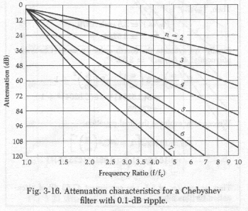
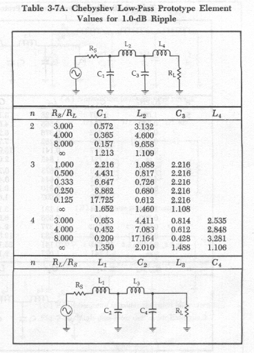
Solution: A low pass filter consists of a ladder network of series L's and shunt C's. Lumped filters are designed by using a set of filter tables. The books by Bowick and Mattheai et. al. tabulate the normalised component values for Chebyshev (maximal attenuation in the stop-band), Butterworth (maximally flat amplitude in the pass-band) and Bessel (most linear phase in the pass-band). These values are normalised according to frequency and terminating impedance. In this project we'll more than likely want the maximum attenuation and so Chebyshev will be the choice.
We see that we need a filter whose response already achieves an attenuation of -30 dB at 58/50 = 1.16 from the f3dB frequency. These books also plot out the absolute values of the transfer functions. The choice boils down to picking the number of combined L and C elements (poles) for the right set of filters of a given ripple. A filter with n = 7 pretty much does the job.
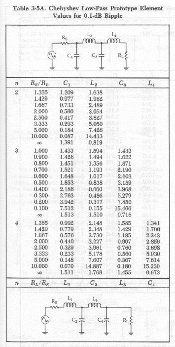
The normalised components taken from Bowick are as follows..
C1' = 1.262L2' = 1.520
C3' = 2.239
L4' = 1.68
C5' = C3'
L6' = L2'
C7' = C1'
Note the enumeration scheme being used with capacitors and inductors given sequential values. The component values are then calculated from the following formula:
C = C'/2/pi/fc/ZoL = Zo*L'/2/pi/fc
The filter is symmetric so that some component values are the same. The transfer function and input impedance have been computed in an matlab file and solve for you to download. Note the sharp attenuation characteristic and the fact that the input impedance remains close to 50 &Omega in the pass-band.
The following component values result C1 = 81pF, C3 = 140pF, L2 = 242nH and L4 = 267nH
Comments on Building the Low Pass Filter
Lumped or discrete filters are the simplest, cheapest and most compact to build. If you want a high Q, the inductors can be wound using one or two silver plated strands of the centre conductor of LM100 50 &Omega coaxial cable using the formula for the inductance of a coil . However any old wire will probably do here. I can also obtain some discrete commercially available conductors that may do the job. In choosing the capacitors be sure to use ceramics or silvered mica and to keep the leads short especially on the higher (140 pF) caps.
Since the low pass and band pass filters are wide band they are not so sensitive to component tolerances and there will be no need to make them tunable. The main disadvantage will be connecting the input and output BNC or N-type connectors into the filter in a way which does not modify the response. The high frequency response of the components however will still be a problem. It will therefore be well worth the effort to investigate the effect of strays in the above matlab model.
The Band Pass Filter
Here I describe how to produce the band pass filter: the details can be found in Bowick's book. A band pass filter is specified by its type (Chebyshev etc), its pass band ripple and source and load impedances in the same way as a low pass filter. In fact band pass filters are directly derived from a low pass design given its 3 dB frequency bandwidth, B and the bandwidth BX, for a certain stop band attenuation, X.
The procedure is as follows. The first step is to design a low pass filter from this information. This is because the design tables are applicable to low pass filter types. Given the type, ripple and source and load impedances we still need to choose the order of the filter (number of elements). All we do is choose the order which gives us the same stop attenuation, X at the normalised frequency given by BX/B. The centre frequency of the bandpass filter is defined to be fo = (f1f2)1/2 where f1 and f2 are the 3 dB frequencies of the bandpass filter. Note also that fo = (f1Xf2X)1/2 applies where f1X and f2X are the X dB frequencies of the bandpass filter.
We then draw out the low pass filter and assign the normalised component values as was previously done in the low pass example. Next we replace all the shunt C's with parallel resonant L and C tank circuits and all the series L's with a series resonant L and C. circuits.
The parallel elements are then calculated from
C = C'/(2 &pi ZoB)L = ZoB/(2 &pi fo2L')
Note that the normalised C' and L' here have the same numerical value. The series elements can be calculated from
C = B/(2 &pi fo2 Zo C')L = ZoL'/(2 &pi B)
And again the normalised C' and L' here have the same numerical value. Note that in each pair, one component is chosen for a low pass filter with a cutoff equal to B while the other is chosen to resonate with it at fo. Thus if B and fo are very different then one component will be very large in value for a circuit operating at fo. This occurs for narrow bandpass filters and the problem is that some components may be too large to realise at high frequencies. We need a different design technique for narrowband bandpass filters.
A Narrowband BandPass Filter
The technique for the design of a bandpass filter as presented by Bowick does not work if the bandwidth is a small fraction of the centre frequency. This is clear to see as in the band pass part of the design, we use the design condition of a low pass filter yet the centre frequency is given by resonating the L's and C's in the same leg. For narrowband filters this can be problematic as it leads to unrealisable component values.
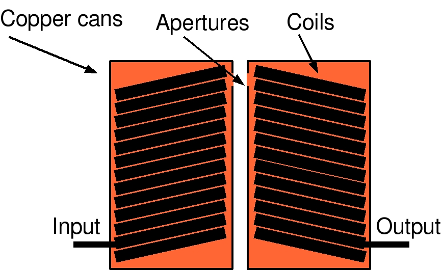
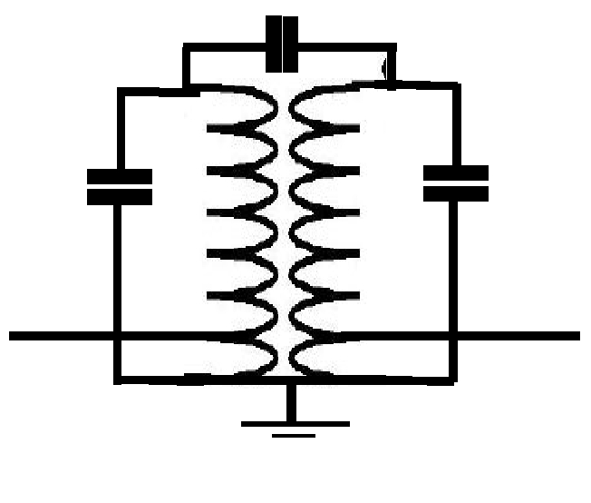
One class of filters that work best when narrow band are the LC resonators (and their distributed half siblings, the helical resonators). Physically they are easy to understand in their operation as shown in the following figure which shows a single stage helical resonator. A helical resonator is simply a pair of high Q coils which are fed at their bases usually by tapping into a low turn. The coils are normally housed in conducting cans with a small opening near their tops. A small amount of stray capacitance leaking through the hole is all that is takes to couple the filters.
The helical resonator is a very popular filter at
HF and VHF because it exploits the slow wave transmission line
structure of the coil helix to obtain standing wave resonances at
relatively low frequencies. The lumped equivalent of this device is
shown in the following figure. Note that there is now a capacitor
which couples energy between the coils. In this circuit the coils are
not in slow wave transmission line resonance like they are when
operated as a helical resonator. The parallel shunt capacitors in the
input and output circuits produce the desired resonance when
resonating with the transformer coils.
How to Design an LC Resonator
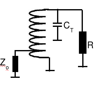
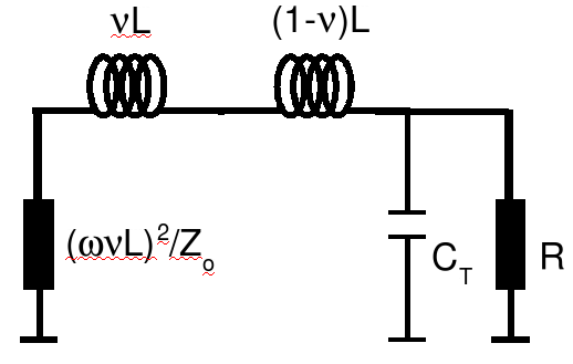
We are now going to do a simple derivation of a few formulae that will allow us to design an LC resonator bandpass filter. The following is the circuit schematic of the filter. It is just a matching network from Zo=50 Ohm to Zo=50 Ohm. It has two back to back auto transformers each with a pair of tuning capacitors. Finally there is a coupling capacitor that bridges the two networks.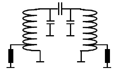
Recall that when we analysed T and PI matching networks, we split the circuit in halves and replaced the break with a resistor to ground. Let's do the same here only we place that resistor in the middle of the coupling capacitor as follows.
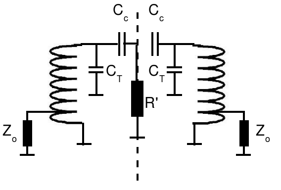
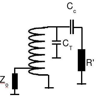
The first thing to do is get rid of the coupling capacitor by absorbing it into the tuning cap. After a little algebra to transform the series combination of Cc and R' to a parallel combination,
R=R' + 1/(&omega 2Cc2R') and Cc -> Cc/(1+&omega CcR')
where Cc has been absorbed in CT. Thus we simply to the following,
Note that we have eliminated Cc from the design path. This may seem strange since it is obvious that it cannot be neglected. However we shall soon see that what has happened is that we have segregated Cc as a separate design variable that does not impinge on any of the other design variables (about to be derived).
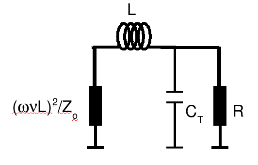
The next step is to simplify the autotransformer but first we have to learn a bit about them. Recall that we can represent any transformer with the following simple circuit.
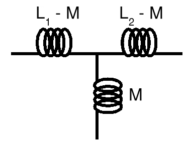
In an autotransformer the primary voltage V1 = &nu V2, where &nu is the turns ratio. As a result it is easy to show that M = &nu L, where M is the mutual inductance and L is the inductance of the whole transformer. The following results,
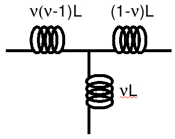
and hence our circuit becomes,
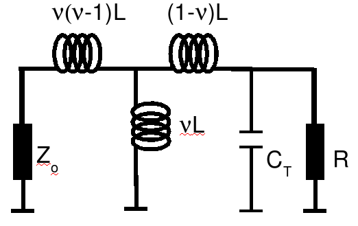
Just one more simplification is necessary before we can do our L-circuit match technique. We know that in order to get a high Q in such a circuit, Zo >> &omega &nu ( &nu - 1 ) L. Thus we may write,

Now let's apply the matching technique. First express the left leg as a series circuit using the above approximation,
or simply,
Now we can apply the L-matching technique. Notice first that we do not know R. This sounds like an impossible situation, but a few moment's thought reveals that it allows us to choose Q. We therefore have the following equation for R instead,
R = (&omega &nu L)2(1 + Q2)/Zo = (&omega &nu L)2Q2/Zo
where the second equality holds if Q>>1. Now from the technique for matching such a circuit,
Q = &omega CT R = (Zo &omega L)/(&omega &nu L)2 = Zo/(&omega L &nu2)
From these two previous equations we finally obtain,
L = Zo/(Q &nu 2 &omega ) and &omega 2 CT L=1
These are our design equations and are all we need. The first step us to choose Q, &nu and the centre frequency of the filter. Usually Q will be in the range 10 - 100 and 0.01 < &nu < 0.5 (approx). The higher is Q, the sharper the response and the steeper the skirts of the filter. Finally experiment with a few values of Cc.
Exercise. This has been implemented in LC resonator model and its solve. Download these and experiment with the influence of varying Cc. Note the interplay between &nu and Cc.
One of the important things to notice in the above exercise is that you can rest assured that your filter model is going to work if the values for L, CT and Cc are reasonable. Thus if you pick a high Q and L turns out to be 10 &mu H, then the filter may not work as expected.Alternate Narrowband Filter Design
For lower Q designs it is possible to reduce the complexity of the LC-resonator filter somewhat as follows.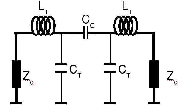
Here the autotransformer has been eliminated in favour of an off the shelf inductor. For analysis, we again divide the circuit into two halves,

Where the 2Cc is the divided coupling capacitor. We then absorb Cc as follows,
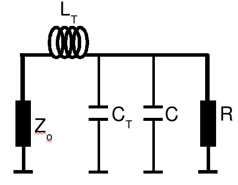
where C = 2Cc/(1 + (2&omega Cc R)2). We can already proceed as per usual by choosing Q. Then
R = Zo(1 + Q2),C+CT = Q / (&omega R),
LT = Q Zo/&omega .
This is all there is to the design procedure but once again Cc has been removed from the design flow, so it has to be guessed and the filter response optimised using solve: LC_PRESELECTOR.m and solve_LC_PRESELECTOR.m.
Finally notice that once a suitable design has been found, and a new calculation for a new frequency fnew=fold/r has to be found then the frequency can be scaled according to, LT=rLT, CT=rCT and Cc = rCc where r is the frequency ratio. This means that the coupling capacitor only has to be guessed for one design.
MATLAB CODE FILTER EXAMPLES
Have a look at the following examples for some clues on the calculation of filter transfer functions
Ex. 11
- Design a Chebyshev (1 dB ripple) bandpass filter with a 3 dB bandwidth from 27 - 54 MHz providing 30 dB of attenuation at 40 Mhz BW and matching from 50 to 50 Ohms.


- Model the above filter in MATLAB and compute the input impedance and the transfer function.
- Using the VNA, source the C's and construct the L's
- Construct the filters and using the tracking generator feature on the spectrum analyser compare with the MATLAB computation. Can you explain any differences?