THE TRANSISTOR AT RADIOFREQUENCY
The project requires the design of RF amplifiers that could be used in several places. A small signal circuit model is simply one described by a circuit model containing linear elements and linear voltage and current sources. Design of small signal RF transistor amplifiers is basic to the design of the power amplifier. A small signal transistor amplifier may also be necessary to couple the mixer output after the Low Pass Filter to the power amplifier. The local oscillator involves the design of a Klapp Voltage Controlled Oscillator which also uses an RF transistor. In this chapter we look at how to do the rf design of an rf amplifier based on an NPN bipolar junction transistor. The following chapter does the same for oscillator design
In previous courses we studied in detail the MOTOROLA MRF157 bipolar junction transistor. However, this transistor is obsolete. Instead, we will look at the relatively easily available and low cost BF199 NPN bipolar junction transistor by Philips as an example of a small signal RF transistor. These devices can be obtained from Farnell for about $1. The information on the web about s-parameters (the crucial information that you need for rf design) is sparse and seemingly inconsistent for the BF199. I have used my usual technique of first principles modelling to predict the s-parameters.
The BF199 is ideal for HF and VHF designs. The datasheet pointed to by the link describes the basic information only about the transistor, such as pinouts, quiescent or DC operating voltages and currents and absolute maximum ratings. Make sure that you read this first.
One unfortunate consequence of this choice is that should one decide to a UHF (>300 MHz) or microwave design then care should be exercised in the application of this transistor (however have a read of this). We'll have a look at the performance in a minute, but students doing UHF and microwave synthesiser design may like to choose another transistor for this purpose. Alternatively they could consider some of the many TV tuner chips.
You have probably seen the low frequency small signal equivalent circuit of a transistor. The following figure shows what the equivalent circuit of a trasnistor looks like at RF. Note the complexity of the circuit. The R,L and C components are parasitic and arise from the physics of the transistor's construction. The current gain b which expresses the output collector current Ic in terms of Ib is just the low frequency value (from the datasheet this has a minimum value of 38 for the BF199). The high frequency behaviour is determined by how the parasitic R,L and C's affect the electrical performance. Sometimes you'll be better off supressing them with well determined external values (if this is possible) just to make a design more reliable, but for the most part we just do our designs taking them into account.
There are just three parameters we need to characterise the RF transistor.
- Firstly the current generator bIb results from the current in the input resistance Rbe. The parameter b is the DC current gain of the tranmsistor and is readily available from datasheets.
- Secondly, the frequency limit of useful operation of the transistor is expressed by fT, the gain-bandwidth product. For the MRF571 it is about 8 GHz. For the BF199 the transition frequency is stated to be 550 MHz. For the NE68519 it is 12GHz. Finite fT, arises from the shunting of the base current by the base-emitter capacitor Cbe. However it is fT and not Cbe which is given by datasheets. At fT, the current flowing in Rbe leads to a collector current equal to Ib or, b = 2pfT RbeCbe or 1 = 2pfT reCbe
- Thirdly, we also need the collector to base feedback or MIller capacitance, Cbc which can cause instability and hence oscillation because it feeds a portion of the output signal back to the input. This is given by datasheets.
The transistor leads give rise to a small inductance on each port. Their effect is significant.
These parameters all depend on the quiescent voltages and currents in the transistor (except of course the lead inductance). The main thing of interest to the designer are the S-parameters of the transistor taken as a four port network with the base-emitter at the input and the collector-emitter at the output. The data for the s parameters of the BF199 listed in the table on this site has been obtained by measurements and also by calculation using SPICE. Unfortunately the two sets of data to not agree too well leaving us confused about how to deal with BF199 RF modelling.
MRF571 and MRF571 provide values for each of the above parameters and a whole lot more. By the way, the MATLAB program provides the S-parameters for MOTOROLA's MRF571 transistor.
The MATLAB program plots the S-parameters as a function of frequency using the parasitic element values (you have to check that the right values are being used in the program!). The datasheet only mentions the feedback or Miller capacitance Cbc = 0.5 pF. The values I used are Re = 25b/Ic0 where b = 40-100, is the low frequency current gain and Ic0 = 7 mA is the quiescent collector current, Cbe = 50 pF, Cbc = 0.5 pF, Lb = Le = Lc = 1.5 nH, Rbb = 0. These parameters are for the quiescent condition Vce = 10V. These quiescent parameters are set by the biasing circuit for the transistor. As can be seen the user is free to choose the values subject to the fact that they do not exceed the absolute maximum ratings of the transistor. The crucial parameter that gives agreement is the input capacitance Cbe = 50 pF. This value is much larger than for the MRF571 (1.3 pF) and explains the inferior high frequency performance of the BF199. Having said this I simply guessed this value in order to give best agreement with the measurements. I also assumed that lead inductance would not differ from that for the MRF157.
The program may be used in the design work so download it and take it for a run. Note that the S-parameters are qualitatively similar to those tabulated in the data for similar conditions. Or should I say that my values disagree at least as well as theirs. Note also that a few of the measured parameters have been arbitrarily set to zero so avoid these
The approach I took above is simple and what I would call the physicist's approach to the problem of parameter estimation. There are just a few parameters that determine the performance of a transistor at radiofrequency. These are Cbe, Cbc, Rbb, Rbe, the DC current gain and the lead inductances. All but the capacitances are pretty much easy to "guesstimate": the DC current gain comes from the datasheet. If you have access to a few experimental measurements of the s-parameters for the transistor at just one or two frequencies you can use the model to obtain the capacitances and hence the s-parameters at all frequencies.
The book by Bowick has an excellent chapter on small signal RF transistor design. The following is a condensed description of that chapter. Since I emphasize the use of the y-parameters in solve.m, I will present the design formulae in this context. An equivalent description in terms of the S-parameters is also possible. Of course given either y or s-parameters one can calculate the other
SMALL SIGNAL RF DESIGN
(1) The case where the transistor is unconditionally stable
The first thing to worry about with a transistor at radiofrequency is stability. There is nothing worse than trying to build a transistor amplifier only to find that it oscillates. The stability of a transistor can be specified in terms of the y-parameters through the Linvill stability factor, C
C = |yfyr|/( 2gigo - real(yfyr) )where gi and go are the real parts of yi and yo. The transistor is unconditionally stable at any frequency for which C < 1. This means that the transistor does not care about its load or source impedance in the absence of external feedback.
Regardless however, a transistor can still be used to make a stable amplifier if the source and load impedances are appropriately chosen. In the presence of a source and load impedance the stability of a transistor can be specified by the Stern stability criterion,
K = 2(gi + Gs)(go + Gl) /(|yryf| + real(yfyr))where Gs and Gl are the source and load conductances and gi etc are the real parts of yi etc. The transistor circuit is stable if K > 1. In the event that the transistor circuit turns out to be unconditionally stable, the Gs and Gl are chosen for a conjugate match (ie max power transfer). Assuming that the transistor is unconditionally stable then one can calculate the maximum available gain, MAG as follows,
MAG = |yf|2/4gigoMaximum available gain is useful for estimating the limiting amplifier power gain.
In the event that the transistor circuit is stable, then one can employ the following formulae to deduce the source and load admittances that must be seen by the transistor for maximum power transfer.
GS = ( [2gigo - real(yfyr)]2 - |yryf| 2 )1/2/ 2goBS = -bi + imag( yfyr )/2go
GL = ( [2gigo - real(yfyr)]2 - |yryf| 2 )1/2/ 2gi
BL = -bo + imag( yfyr )/2gi
and
YS = GS + jBS
YL = GL + jBL
where YS and YL yield the conjugate match. The source and load susceptances bi etc are the real parts of yi etc. Given these we can go back to the Stern criterion and check stability.
Finally, if we manage to find a GS and GL that are stable, then we can proceed to find the power gain of the amplifier stage, the transducer gain,
GT = 4GSGL |yf|2/ | (yi + YS)(yo + YL) - yf yr |2Thus the procedure for the design of an amplifier at a certain frequency for an unconditionally stable transistor is as follows,
(1) Obtain the y-parameters at this frequency or estimate them from the S-parameters or the circuit model above using the MATLAB program
(2) Check if the transistor is unconditionally stable using the Linvill criterion (C < 1). Proceed only if it is.
(3) Use the MAG formula to check the max power gain the transistor circuit can provide.
(4) Use the conjugate matching formula to determine the source and load admittances for maximum power transfer.
(5) Use the matching techniques to match the transistor to the actual source and load impedancesa of the circuit.
(6) Use the Stern criterion to confirm circuit stability (K > 1 everywhere) over the whole frequency range.
(7) Compare the computed power gain with the transducer gain.
Note that there is a choice of y-parameters depending on the circuit biasing (esp. Vce and Ic). Thus if the y-parameters indicate that the transistor is not unconditionally stable, change the bias (but this has to work for all frequencies). This may also be necessary if step (6) fails.
ExampleA transistor has the following Y parameters at 100 MHz with Vce =10 Volts and Ic = 5 mA.
yi = 8 + j5.7 mmhosyo = 0.4 + j1.5 mmhos
yf = 52 - j20 mmhos
yr = 0.01 - j0.1 mmhos
where a mmho is a milliMHO (said Larry to Curly).
From the Linvill criterion we obtain C = 0.71. Because C < 1 the transistor is unconditionally stable. Otherwise we could never proceed!
The MAG is given by 23.8 dB. We will not be able to achieve a gain greater than this.
YS = 6.95 - j12.41 mmhos.
This is the source impedance that the transistor must see for maximum power transfer. The transistors actual input admittance is the complex conjugate of this number.
For the load,
YL = 0.347 - j1.84 mmhos.The actual output admittance of the transistor is the complex conjugate of this number.
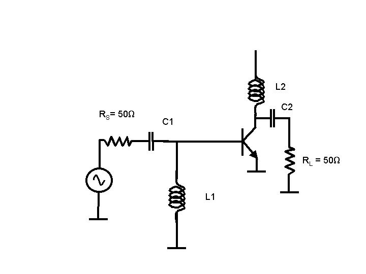
The next step is to design the matching networks for the input and output circuits and this can proceed as in the section on matching. A sample matching circuit is the following.
The above is a small signal equivalent circuit. The final design must include a power supply, decoupling and a bias circuit to set the bias conditions to those which achieve the assumed Y parameters. It is left as an exercise.
(2) The case where the transistor is not unconditionally stableWhat if the transistor is not unconditionally stable? Given the approximate nature of estimating the y-parameters from a circuit model, small changes can lead to incorrect conclusions about unconditonal stability and, even if the transistor is stable at the chosen frequency, it may become unstable elsewhere. What approach do we use in this situation?
In this case we may use several techniques. One is to neutralise the transistor. This means we insert a component from collector to base that cancels or alters the transistor's internal feedback. It is this internal feedback or Miller capacitance that is responsible for the instability. A problem with this technique is that we have to be certain that the instability is mitigated at all frequencies.
Another technique is to employ a matching network that gives sub-optimal power transfer but prevents the transistor from oscillating via the Stern criterion. We will investigate this procedure.
(1) Choose GS based on some criterion e.g. input network Q at the desired frequency of operation.
(2) Select a value of K that gives stability (e.g. K = 3).
(3) Solve for GL from the expression for the Stern Criterion.
(4) Now that GS and GL are determined all that
remains is to determine BS and BL.
Choose BL = -bo. The resultant YL
will be very close to that required.
(5) One can determine the input admittance from, Yin = yi - yryf/(yo + YL)
(6) Set BS = -Bin.
(7) Use the transducer gain GT, to calculate the gain of the stage. Is this OK? If not iterate on GS.
(8) Proceed to match this to the actual source and load impedances at the frequency of interest.
(9) Use the Stern criterion to confirm circuit stability (K > 1) over the whole frequency range.
(10) Compare the computed power gain with the transducer gain.